DS512 January 18, 2006 www.xilinx.com 1
Product Specification
© 2006 Xilinx, Inc. All rights reserved. XILINX, the Xilinx logo, and other designated brands included herein are trademarks of Xilinx, Inc. All other trademarks are the property of their respective
owners. Xilinx is providing this design, code, or information "as is." By providing the design, code, or information as one possible implementation of this feature, application, or standard, Xilinx
makes no representation that this implementation is free from any claims of infringement. You are responsible for obtaining any rights you may require for your implementation. Xilinx expressly
disclaims any warranty whatsoever with respect to the adequacy of the implementation, including but not limited to any warranties or representations that this implementation is free from claims
of infringement and any implied warranties of merchantability or fitness for a particular purpose.
Introduction
The Xilinx LogiCORE™ Block Memory Generator is an
advanced memory constructor, generating area and
performance optimized memories using embedded
block RAM resources in Xilinx FPGAs. Available
through the CORE Generator™ system, the core allows
users to quickly create optimized memories to leverage
the performance and features of block RAMs in Xilinx
FPGAs.
Features
• Generates single-port RAM, simple dual-port RAM,
true dual-port RAM, single-port ROM, dual-port
ROM
• Performance up to 450 MHz
• Supports data widths from 1 to 1152 bits
• Supports memory depths from 8 to 9M words
(limited only by memory resources on selected part)
• Supports configurable port aspect ratios for
dual-port configurations
• Supports read-to-write aspect ratios in Virtex™-4
FPGAs
• Optimized algorithm for minimum block RAM
resource utilization
• Configurable memory initialization
• Supports individual write enable per byte in
Virtex-4 devices
• Optimized VHDL and Verilog behavioral models
for fast simulation times
• Structural simulation models for precise simulation
of memory behaviors
• Selectable operating mode per port: WRITE_FIRST,
READ_FIRST, or NO_CHANGE
0
Block Memory Generator
v1.1
DS512 January 18, 2006
00
Product Specification
LogiCORE Facts
Core Specifics
Supported Device
Family
Virtex-4, Virtex-II Pro, Virtex-II,
Spartan
TM
-3E, Spartan-3
Package All
Speed Grade All
Performance Varied, based on core parameters
Core Resources
Block RAM Varied, based on core parameters
DCM None
BUFG None
IOBs/RocketIO™ None
PPC None
IOB-FF/TBUFs None
Provided with Core
Documentation Product Specification
Design File Formats NGC netlist
Design Tool Requirements
Xilinx Implementation
Tools
ISE 8.1i
Supported
Behavioral Models
VHDL, Verilog
Synthesis XST 8.1i
Support
Provided by Xilinx, Inc.
Block Memory Generator v1.1
2 www.xilinx.com DS512 January 18, 2006
Product Specification
Overview
The Block Memory Generator core uses the embedded Block Memory primitives available in Xilinx
FPGAs, extending the functionality and capabilities of a single primitive to memories of arbitrary
widths and depths. The sophisticated algorithms behind the Block Memory Generator core produce
optimized solutions for a wide range of configurations, providing convenient access to memories opti-
mized for your needs.
The Block Memory Generator has two fully independent ports. The A port has a write and a read inter-
face, as does the B port. These four interfaces access a shared memory space, and can be configured
uniquely for the Virtex-4 architecture. When not using all four interfaces, the user can select a simpli-
fied memory configuration such as Single-Port Memory or Simple Dual-Port Memory, which allows
the core to more efficiently use the available resources.
For users familiar with the Single-Port Block Memory and Dual-Port Block Memory cores, the Block
Memory Generator is not fully backwards compatible with these cores. The differences are discussed in
"Revision History" on page 46.
Applications
The Block Memory Generator core is used to create customized memories to suit any application. Typ-
ical applications include:
• Single-Port Memory: Processor scratch RAM, very large look-up tables.
• Dual-Port Memory: Content addressable memories, FIFOs, multi-processor storage.
• Read-Only Memory: Program code storage, initialization ROM.
Feature Summary
Memory Types
The Block Memory Generator core uses embedded block RAM to generate the following types of mem-
ories:
•Single-port RAM
• Simple dual-port RAM
• True dual-port RAM
•Single-port ROM
•Dual-port ROM
For dual-port memories, each port operates completely independently. Operating mode, clock fre-
quency, and optional pins are selectable per port.
Selectable Memory Algorithm
The core concatenates block RAM primitives according to one of the following algorithms:
• Minimum Area Algorithm: The memory is generated using the minimum number of block RAM
primitives. Both data and parity bits are utilized.
• Selectable Primitive Algorithm: The memory is generated using only one type of block RAM
primitive. For a complete list of primitives available for each device family, see the data sheet for
that family.
Block Memory Generator v1.1
DS512 January 18, 2006 www.xilinx.com 3
Product Specification
Configurable Width and Depth
The Block Memory Generator can generate memory structures from 1 to 1152 bits wide, and at least
eight locations deep. The maximum depth of the memory is limited only by the number of block RAM
primitives in the target device.
Selectable Port Aspect Ratios
The core supports the same port aspect ratios as the block RAM primitives:
• In all supported device families, the A port width may differ from the B port width by a factor of 1,
2, 4, 8, 16, or 32.
• In Virtex-4 FPGA-based memories, the read width may differ from the write width by a factor of 1,
2, 4, 8, 16, or 32 for each port. The maximum ratio between any two of the data widths (
DINA,
DOUTA, DINB,
and DOUTB) is 32:1.
Memory Initialization
The memory contents can be optionally initialized using a memory coefficient (COE) file or by using
the default data option. A COE file can define the initial contents of each individual memory location,
while the default data option defines the initial content of all locations.
Selectable Operating Mode per Port
The Block Memory Generator supports the block RAM primitive operating modes: WRITE FIRST,
READ FIRST, and NO CHANGE. Each port may be assigned an operating mode.
Optional Output Registers
The Block Memory Generator provides two optional stages of output registering to increase memory
performance. The core supports the Virtex-4 embedded block RAM registers as well as registers imple-
mented in the FPGA fabric.
Optional Synchronous Set/Reset Pin
The core provides optional set/reset pins (SSRA and SSRB) pin per port that synchronously initialize
the read output to a programmable value.
Optional Enable Pin
The core provides optional port enable pins (ENA and ENB) to control the operation of the memory.
When deasserted, no read, write, or reset operations are performed on the respective port. If the enable
pins are not used, it is assumed that the port is always enabled.
Optional Byte-Write Enable
In Virtex-4 FPGA-based memories, the Block Memory Generator core provides byte-write support for
memory widths of 9-bit multiples.
Functional Description
The Block Memory Generator is used to build custom memory modules from block RAM primitives in
Xilinx FPGAs. The core implements an optimal memory by arranging block RAM primitives based on
user selections, automating the process of primitive instantiation and concatenation. Using the CORE
Block Memory Generator v1.1
4 www.xilinx.com DS512 January 18, 2006
Product Specification
Generator graphical user interface (GUI), the user can configure the core and rapidly generate a highly
optimized custom memory solution.
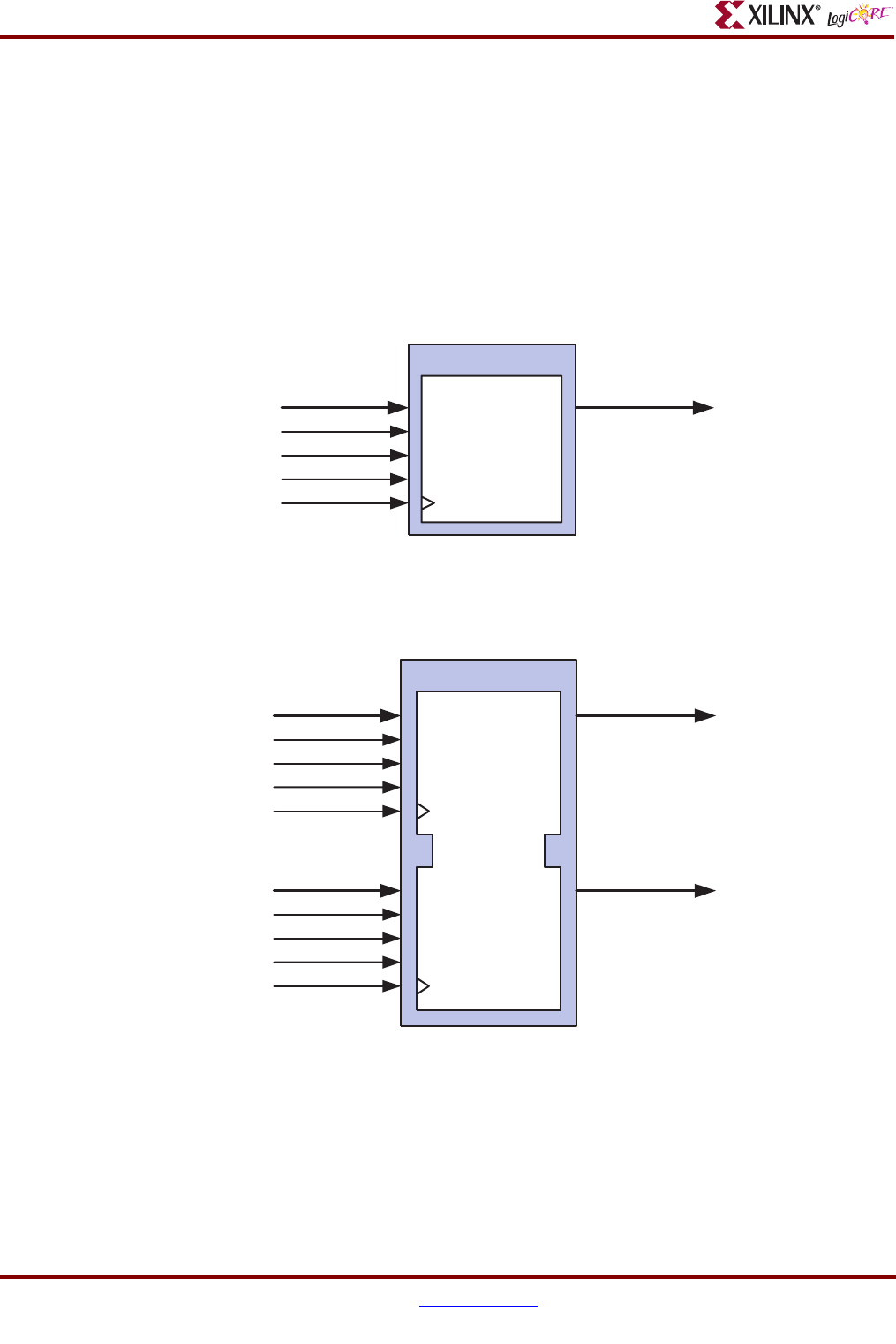
Memory Type
The Block Memory Generator core can create five types of memories: Single-port RAM, Simple
dual-port RAM, True dual-port RAM, Single-port ROM, and Dual-port ROM. Figures 1 through 5 illus-
trate the signals available for each memory type. Optional pins are shown in italics.
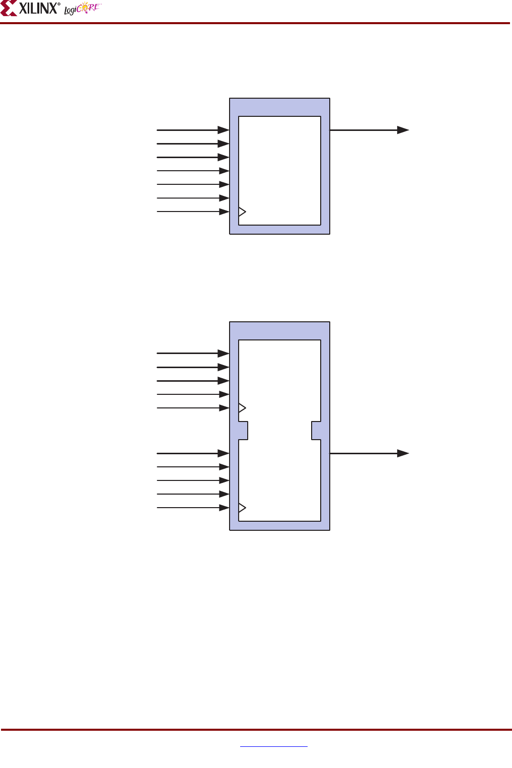
The single-port ROM allows read access to the memory space through a single port, as shown in
Figure 1.
The dual-port ROM allows read access to the memory space through two ports, as shown in Figure 2.
Figure Top x-ref 1
Figure 1: Single-port ROM
Figure Top x-ref 2
Figure 2: Dual-port ROM
Single-Port ROM
ADDRA
ENA
SSRA
CLKA
DOUTA
REGCEA
Dual-Port ROM
ADDRA
ENA
SSRA
CLKA
DOUTA
DOUTB
REGCEA
ADDRB
ENB
SSRB
CLKB
REGCEB
Block Memory Generator v1.1
DS512 January 18, 2006 www.xilinx.com 5
Product Specification
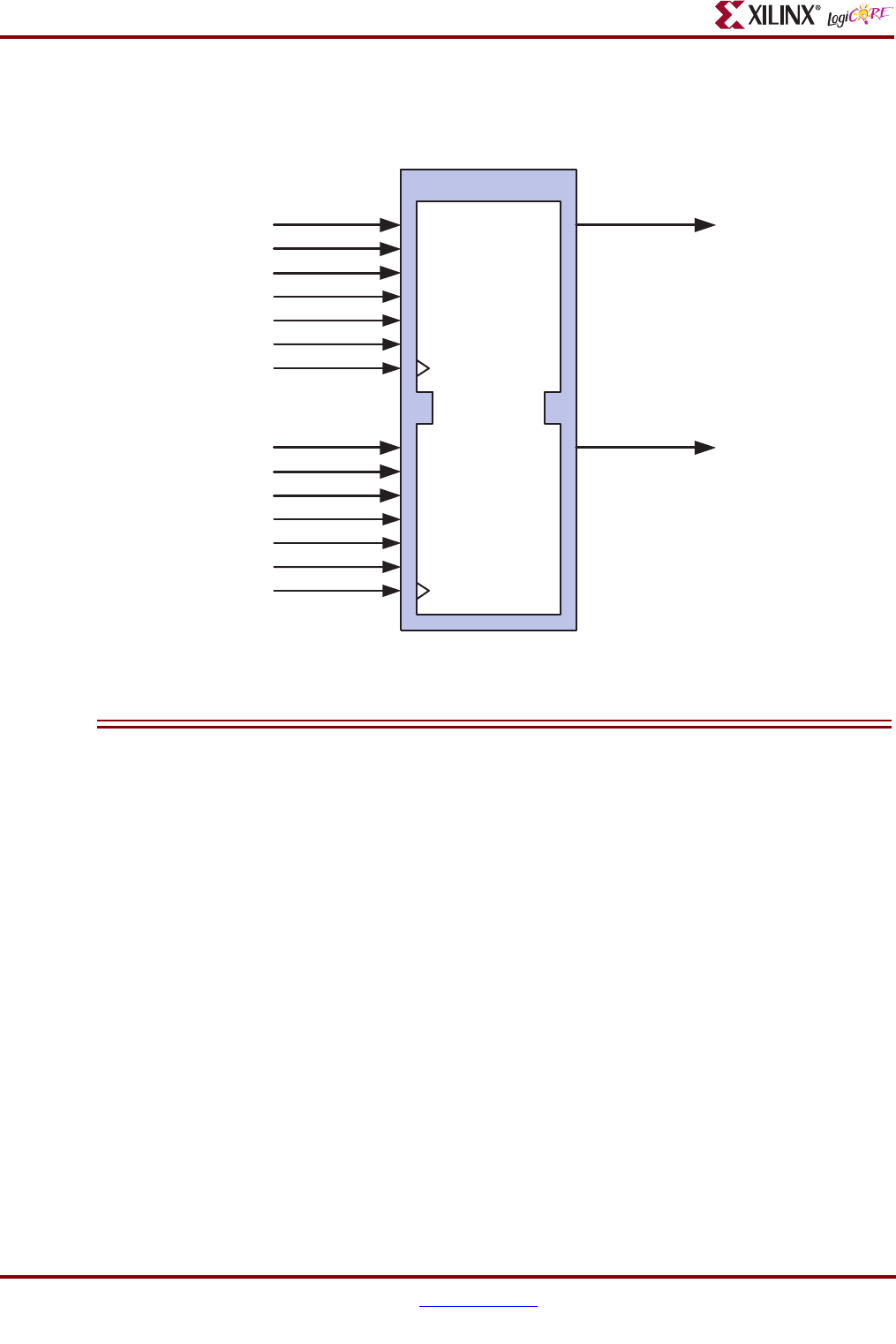
The single-port RAM allows read and write access to the memory through a single port, as shown in
Figure 3.
The simple dual-port RAM shown in Figure 4 provides two ports, A and B. Write access to the memory
is allowed via port A, and read access is allowed via port B.
Figure Top x-ref 3
Figure 3: Single-port RAM
Figure Top x-ref 1
Figure 4: Simple Dual-port RAM
Single-Port RAM
ADDRA
DINA
ENA
WEA
SSRA
CLKA
DOUTA
REGCEA
Simple Dual-Port RAM
CLKA
DOUTBADDRB
ENB
SSRB
CLKB
REGCEB
ADDRA
DINA
ENA
WEA
Block Memory Generator v1.1
6 www.xilinx.com DS512 January 18, 2006
Product Specification
The true dual-port RAM shown in Figure 5 provides two ports, A and B. Read and write accesses to the
memory are allowed on either port.
Selectable Memory Algorithm
The Block Memory Generator core arranges block RAM primitives according to one of two algorithms:
the minimum area algorithm and the selectable primitive algorithm.
Figure Top x-ref 2
Figure 5: True Dual-port RAM
True Dual-Port RAM
ADDRA
DINA
ENA
WEA
SSRA
CLKA
DOUTA
DOUTB
REGCEA
ADDRB
DINB
ENB
WEB
SSRB
CLKB
REGCEB
Block Memory Generator v1.1
DS512 January 18, 2006 www.xilinx.com 7
Product Specification
Minimum Area Algorithm
The minimum area algorithm provides a highly optimized solution, resulting in a minimum number of
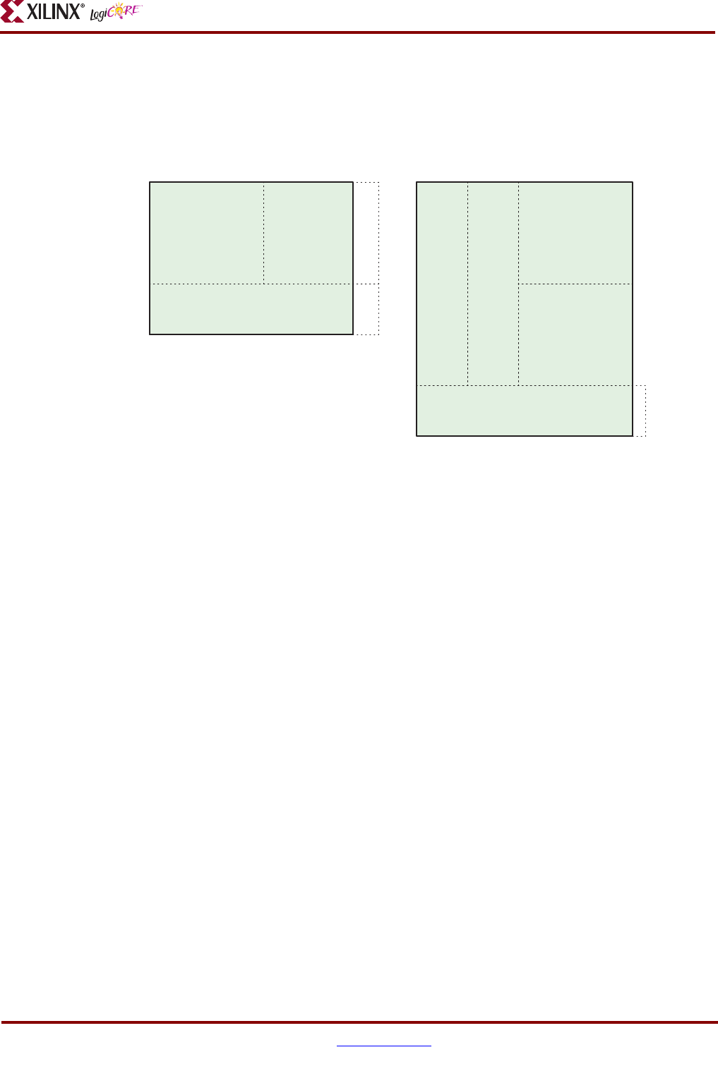
block RAM primitives used, while reducing output multiplexing. Figure 6 depicts two examples of
memories built using the minimum area algorithm.
In the first example, a 16x3k memory is implemented using three block RAMs. While it may have been
possible to concatenate three 18x1k block RAMs in depth, this would require more output multiplex-
ing. The minimum area algorithm maximizes performance in this way while maintaining minimum
block RAM usage.
The second example, a 17x5k memory, further demonstrates how the algorithm can pack block RAMs
efficiently to use the fewest resources while maximizing performance by reducing output multiplexing.
Selectable Primitive Algorithm
The selectable primitive algorithm allows the user to select a single block RAM primitive type. The core
will build the memory by concatenating this single primitive type in width and depth. It is useful in
Figure Top x-ref 3
Figure 6: Examples of the Minimum Area Algorithm
16x3k memory
9x2k
18x1k
9x2k
17x5k memory
4x4k 4x4k
9x2k
9x2k
18x1k
Block Memory Generator v1.1
8 www.xilinx.com DS512 January 18, 2006
Product Specification
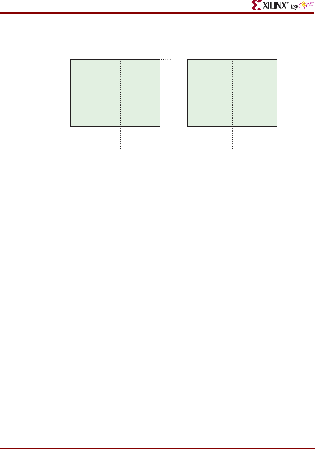
systems that require a fixed primitive type. Figure 7 depicts two 16x3k memories, one built using the
9x2k primitive type, the other built using the 4x4k primitive type.
Note that both implementations use four block RAMs, and that some of the resources utilized extend
beyond the usable memory space. It is up to the user to decide which primitive type is best for their
application.
The selectable primitive algorithm supports all of the block RAM primitive types: 1x16k, 2x8k, 4x4k,
9x2k, 18x1k, and 36x512. In Virtex-4 based memories, the 1x32k cascaded primitive type is also sup-
ported, which cascades two block RAMs primitives in depth using an embedded mux for faster oper-
ation.
When using data width aspect ratios, the primitive type dimensions are chosen with respect to the A
port write width. Note that primitive selection may limit port aspect ratios as described in "Aspect
Ratio Limitations" on page 12. When using the byte write feature, only the 9x2k, 18x1k, and 36x512
primitive types are available.
Selectable Width and Depth
The Block Memory Generator generates memories with widths from 1 to 1152 bits, and with depths of
8 or more words. The memory is built by concatenating block RAM primitives, and total memory size
is limited only by the number of block RAMs on the target device.
Write operations to out of range addresses are guaranteed not to corrupt data in the memory, while
read operations to out of range addresses will return invalid data. Note that the set/reset function
should not be asserted while accessing an out of range address – it will also result in invalid data on the
output.
Operating Mode
The operating mode determines which data word is presented on the output during a write operation.
Each port is assigned an operating mode. The Block Memory Generator supports the three operating
modes supported by the block RAM primitives. These operating modes are described in detail below.
For more information, refer to the Block RAM section of the user guide for the specific device family.
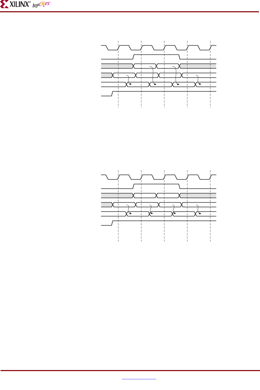
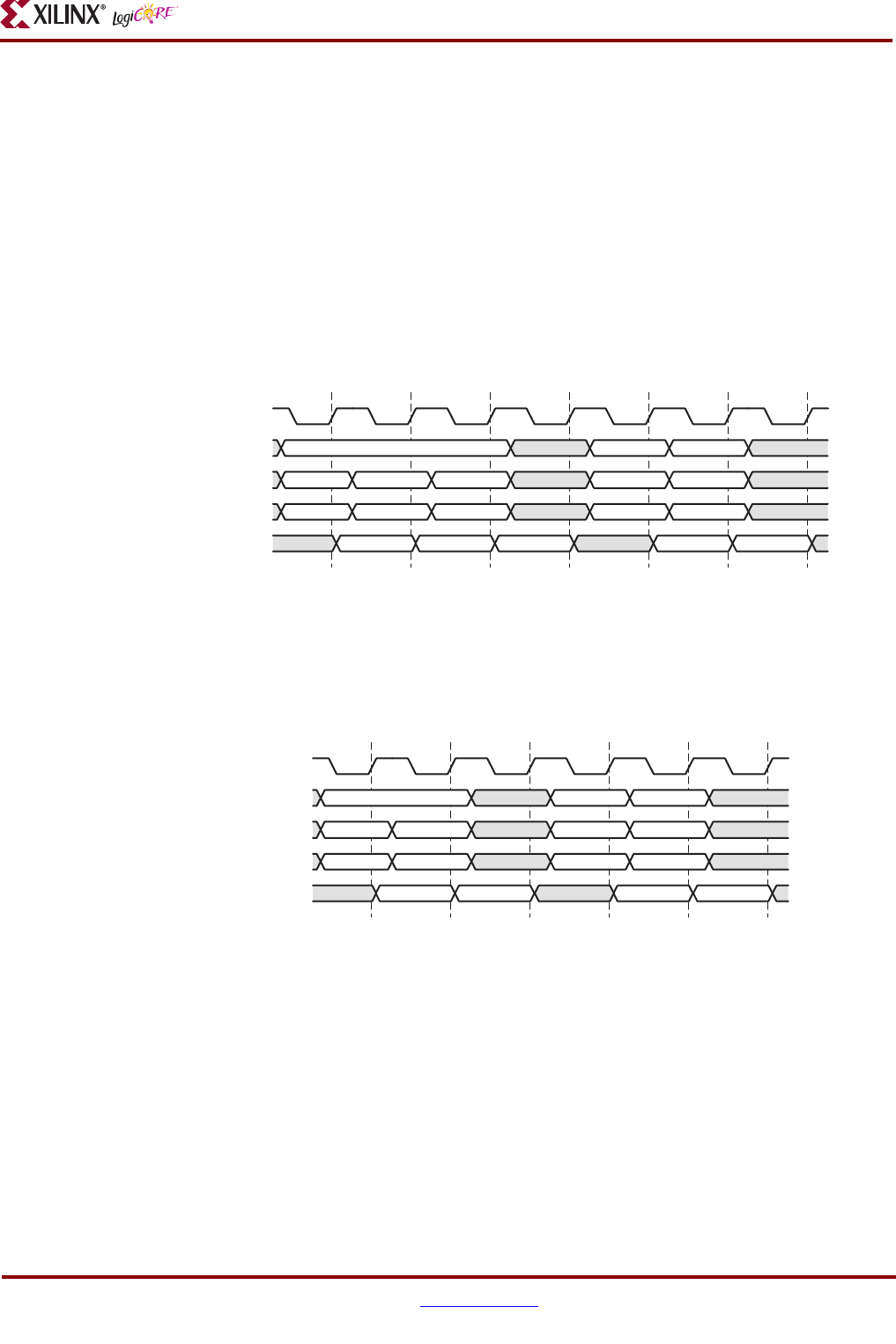
• Write First Mode: In WRITE_FIRST mode, the input data is simultaneously written into memory
and driven on the data output, as shown in Figure 8. This transparent mode offers the flexibility of
Figure Top x-ref 4
Figure 7: Examples of the Selectable Primitive Algorithms
16x3k memory
9x2k
9x2k
9x2k
9x2k
16x3k memory
4x4k 4x4k 4x4k 4x4k
Block Memory Generator v1.1
DS512 January 18, 2006 www.xilinx.com 9
Product Specification
using the data output bus during a write operation on the same port.
Note that the WRITE_FIRST operation for Virtex-4 is affected by the optional read-to-write aspect
ratio and byte-write features. For more details, see "Virtex-4 Write First Mode" on page 12.
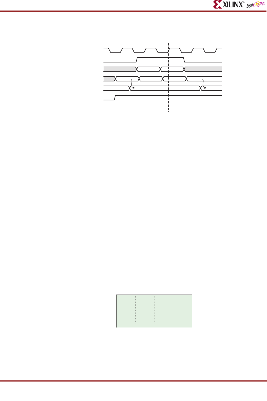
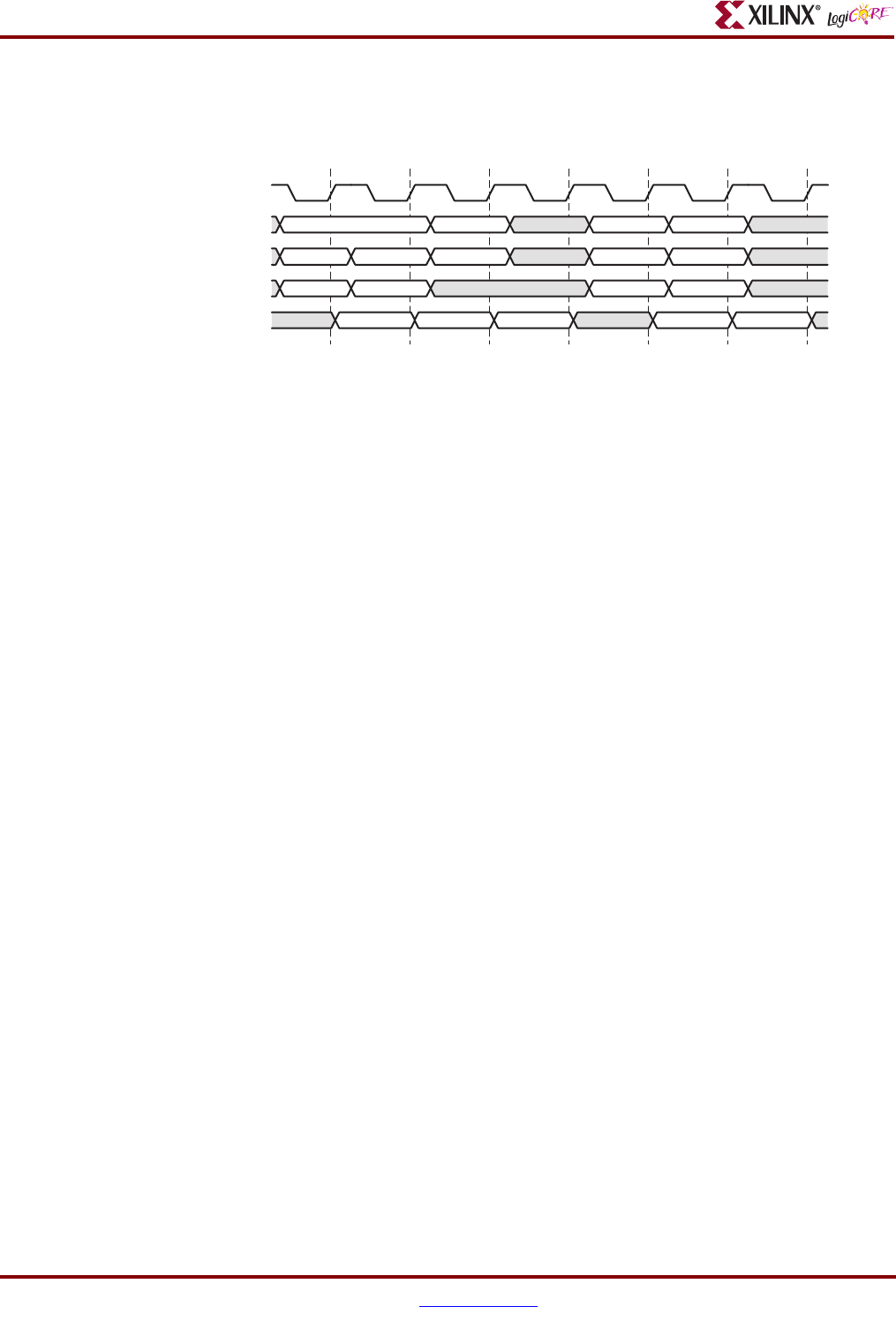
• Read First Mode: In READ_FIRST mode, data previously stored at the write address appears on
the data output, while the input data is being stored in memory. This read-before-write behavior is
illustrated in Figure 9.
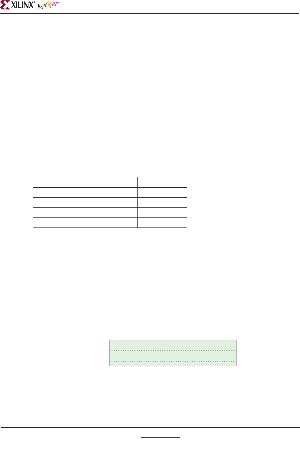
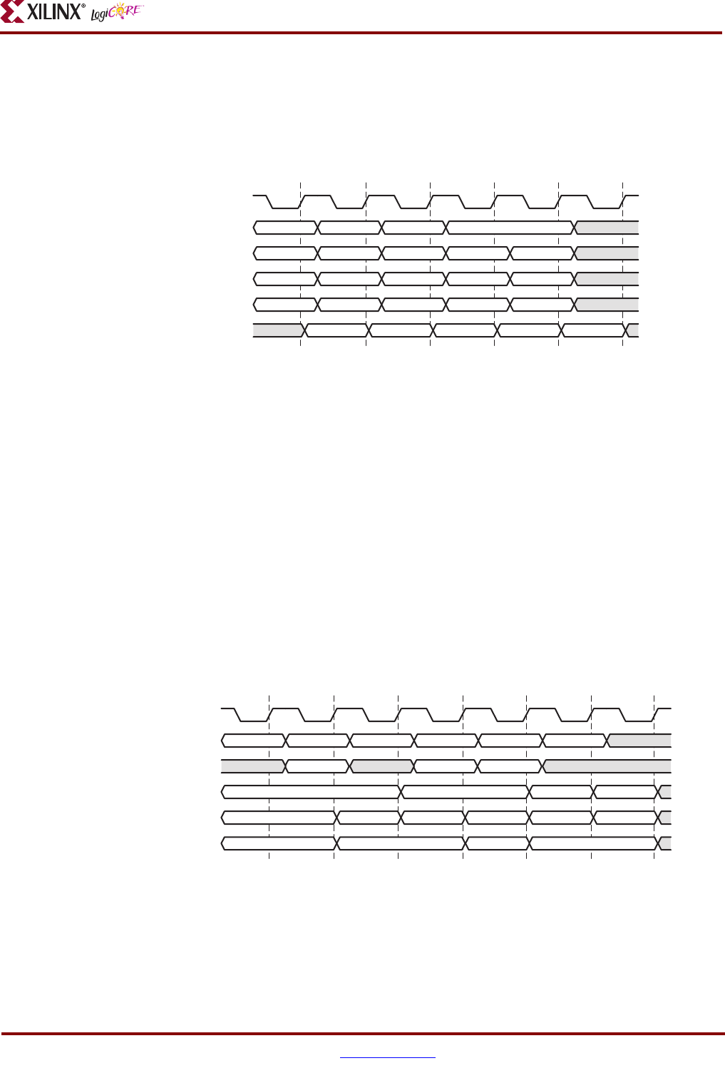
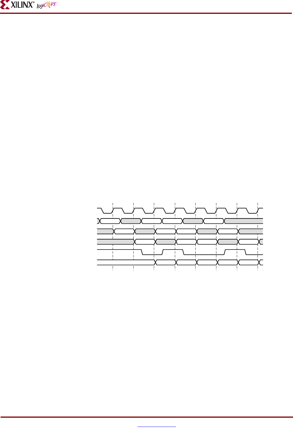
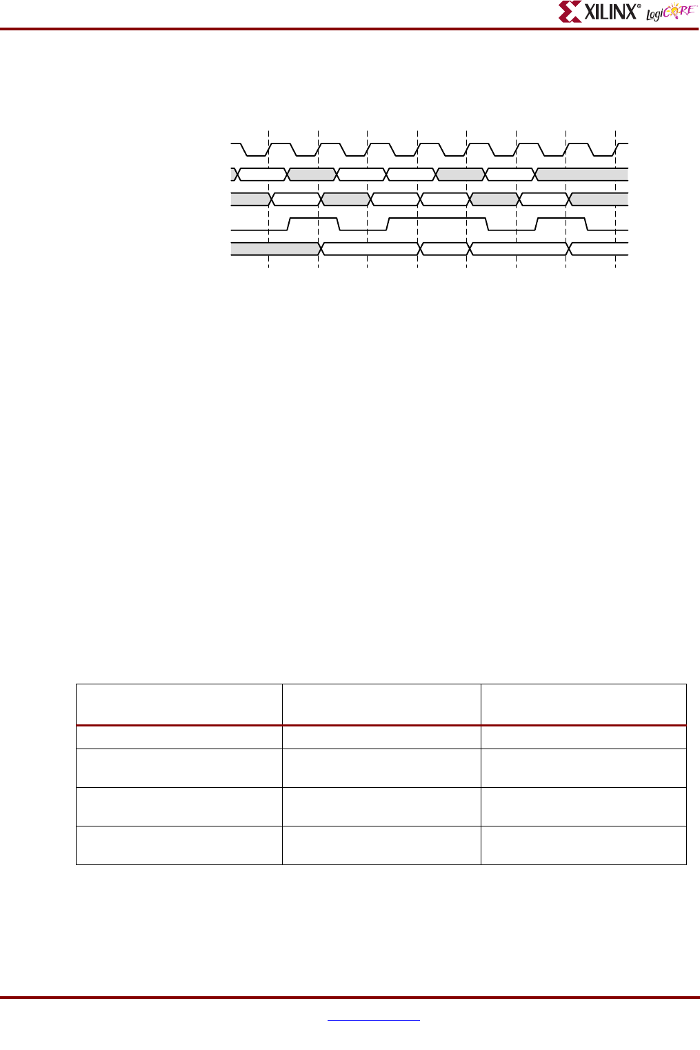
• No Change Mode: In NO_CHANGE mode, the output latches remain unchanged during a write
operation. As shown in Figure 10, the data output is still the previous read data and is unaffected
Figure Top x-ref 5
Figure 8: Write First Mode Example
Figure Top x-ref 6
Figure 9: Read First Mode Example
aa
WEA
DINA[15:0]
DOUTA[15:0]
CLKA
ADDRA
bb
1111
ENA
cc dd
2222
MEM(aa) 1111 2222 MEM(dd)0000
DISABLED READ
WRITE
MEM(bb)=
1111
WRITE
MEM(cc)=
2222
READ
aa
WEA
DINA[15:0]
DOUTA[15:0]
CLKA
ADDRA
bb
1111
ENA
cc dd
2222
MEM(aa) old MEM(bb) old MEM(cc) MEM(dd)0000
DISABLED READ
WRITE
MEM(bb)=
1111
WRITE
MEM(cc)=
2222
READ
Block Memory Generator v1.1
10 www.xilinx.com DS512 January 18, 2006
Product Specification
by a write operation on the same port.
Data Width Aspect Ratios
The Block Memory Generator supports data width aspect ratios. This allows the port A data width to
be different than the port B data width, as described in Port Aspect Ratios. In Virtex-4 FPGA-based
memories, all four data busses (DINA, DOUTA, DINB, and DOUTB) can have different widths, as
described in "Virtex-4 Read-to-Write Aspect Ratios" on page 11.
The limitations of the data width aspect ratio feature (some of which are imposed by other optional fea-
tures) are described in "Aspect Ratio Limitations" on page 12. The CORE Generator GUI ensures only
valid aspect ratios as selected.
Port Aspect Ratios
The Block Memory Generator supports port aspect ratios of 1:32, 1:16, 1:8, 1:4, 1:2, 1:1, 2:1, 4:1, 8:1, 16:1,
and 32:1. The port A data width can be up to 32 times larger than the port B data width, or vice versa.
The smaller data words are arranged in little-endian format, as illustrated in Figure 11.
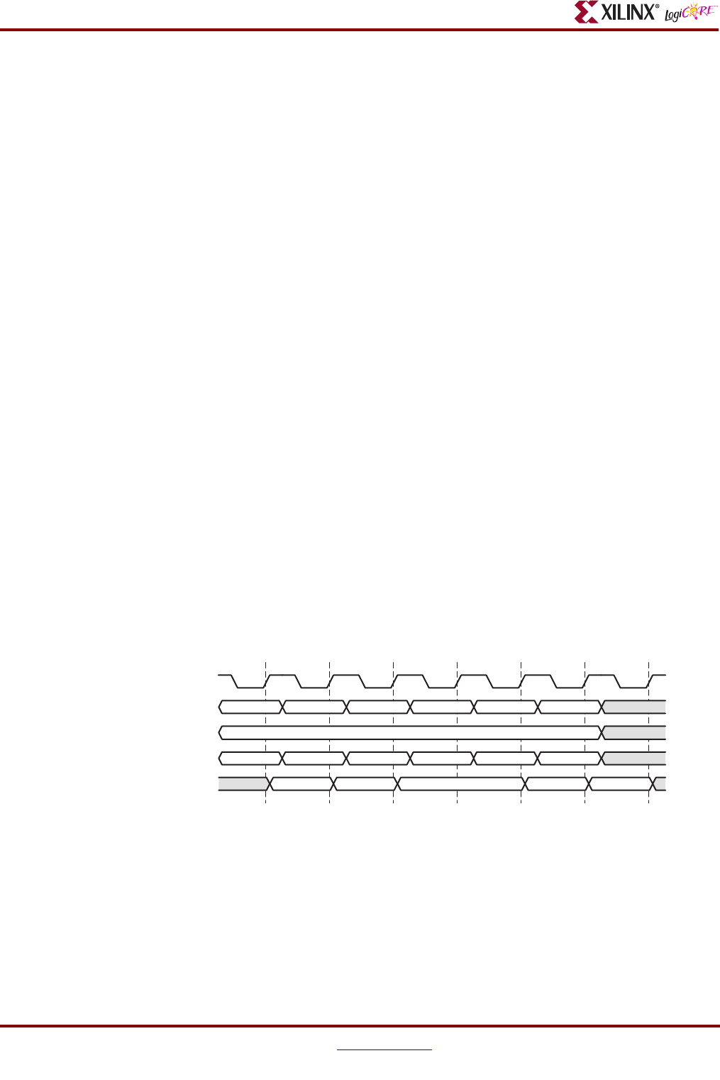
Port Aspect Ratio Example
Consider a true dual-port RAM of 32x2048, which is the A port width and depth. From the perspective
of an 8-bit B port, the depth would be 8192. The
ADDRA bus is 11 bits, while the ADDRB bus is 13 bits.
The data is stored little-endian, as shown in Figure 11. Note that A
n
is the data word at address n, with
respect to the A port. B
n
is the data word at address n with respect to the B port. A
0
is comprised of B
3
,
B
2
, B
1
, and B
0
.
Figure Top x-ref 7
Figure 10: No Change Mode Example
Figure Top x-ref 8
Figure 11: Port Aspect Ratio Example Memory Map
aa
WEA
DINA[15:0]
DOUTA[15:0]
CLKA
ADDRA
bb
1111
ENA
cc dd
2222
MEM(aa) MEM(dd)0000
DISABLED READ
WRITE
MEM(bb)=
1111
WRITE
MEM(cc)=
2222
READ
31 0
B
3
A
0
=
.
.
.
7 0
. .
7 0
. .
7 0
. .
7 0
. .
7 0
. .
7 0
. .
7 0
. .
7 0
. .
B
2
B
1
B
0
B
7
B
6
B
5
B
4
A
1
=
Block Memory Generator v1.1
DS512 January 18, 2006 www.xilinx.com 11
Product Specification
Virtex-4 Read-to-Write Aspect Ratios
When implementing RAMs targeting Virtex-4 FPGAs, the Block Memory Generator allows read and
write aspect ratios. On each port, the read to write data width ratio can be 1:32, 1:16, 1:8, 1:4, 1:2, 1:1, 2:1,
4:1, 8:1, 16:1, or 32:1.
For true dual-port RAMs, the four data busses,
DINA, DOUTA, DINB, and DOUTB, can have different
widths. For single-port RAMs,
DINA and DOUTA widths can be independent. The maximum ratio
between any two data buses is 32:1. The widest data bus can be no larger than 1152 bits.
If the read and write data widths are different, the memory depth is different with respect to read and
write accesses. The depth ratio is the inverse of the width ratio. The address bus must be large enough
to address the deeper of the two depths, since it is shared by read and write accesses. For the shallower,
the least significant bits of the address bus are ignored. The smaller data words are arranged in lit-
tle-endian format, as illustrated in Figure 12.
Virtex-4 Read-to-Write Aspect Ratio Example
Consider a true dual-port RAM of 64x512, which is the A port write width and depth. Table 1 lists the
four data port widths and their respective depths for this example.
The
ADDRA width is determined by the larger of the A port depths (2048). Therefore, ADDRA is 11 bits
wide. On port A, read operations utilize the entire
ADDRA bus, while write operations ignore the least
significant 2 bits.
In the same way, the
ADDRB width is determined by the larger of the B port depths (1024). Therefore,
ADDRB is 10 bits wide. On port B, read operations utilize the entire ADDRB bus, while write operations
ignore the least significant 3 bits.
The memory map in Figure 12 shows how port B write words are related to port A write words, in a lit-
tle-endian arrangement. Note that AW
n
is the write data word at address 'n' with respect to port A,
while BW
n
is the write data word at address 'n' with respect to port B.
BW
0
is made up of AW
3
, AW
2
, AW
1
, and AW
0
. In the same way, BR
0
is made up of AR
1
and AR
0
, and
AW
0
is made up of BR
1
and BR
0
.
Table 1: Read-to-Write Aspect Ratio Example Ports
Interface Data Width Memory Depth
Port A Write 64 512
Port A Read 16 2048
Port B Write 256 128
Port B Read 32 1024
Figure Top x-ref 9
Figure 12: Read-to-Write Aspect Ratio Example Memory Map
BW
0
=
.
.
.
BW
1
=
255 0
AW
3
AW
2
AW
1
AW
7
AW
6
AW
5
AW
4
AW
0
Block Memory Generator v1.1
12 www.xilinx.com DS512 January 18, 2006
Product Specification
In the above example, the largest data width ratio is port B write words (256 bits) to port A read words
(16 bits). This ratio is 16:1.
Aspect Ratio Limitations
In general, no port data width may be wider than 1152 bits, and no two data widths can have a ratio
greater than 32:1. However, some optional features further limit data width aspect ratios:
• Byte-writes: When using byte-writes, no two data widths can have a ratio greater than 4:1.
• Selectable primitive algorithm: When using the selectable primitive algorithm with an N-bit wide
primitive, aspect ratios are limited to 32:N and 1:N from the port A write width. For example, using
the 4x4k primitive type, the other ports may be no more than 8 times (32:4) larger than port A write
width and no less than 4 times (1:4) smaller.
Virtex-4 Byte-Writes
The Block Memory Generator provides byte-write support in Virtex-4 devices. Byte-writes are avail-
able for memories of 9-bit multiples — parity bits are included.
When byte-writes are enabled, the
WE[A|B] bus is N bits wide, where N is the number of bytes in
DIN[A|B]. The most significant bit in the write enable bus corresponds to the most significant byte in
the input word. Bytes will be stored in memory only if the corresponding bit in the write enable bus is
asserted during the write operation.
To remove parity and use 8-bit bytes, the user may tie off the 9th bit of each byte in the data words. The
byte-write feature may be used in conjunction with the Virtex-4 data width aspect ratios. However, it
may not be used with the NO_CHANGE operating mode. The byte-write feature also affects the oper-
ation of WRITE_FIRST mode, as described in
"Virtex-4 Write First Mode" on page 12.
Byte-Write Example
Consider a single-port RAM with a data width of 24 bits, or 3 bytes with parity bits tied off. The write
enable bus,
WEA, consists of 3 bits. Figure 13 illustrates the use of byte-writes, and shows the contents
of the RAM at address 0. Assume all memory locations are initialized to 0.
Virtex-4 Write First Mode
The byte-write feature and the read-to-write data width aspect ratio have special consideration when
using WRITE_FIRST mode in Virtex-4 FPGAs. In general, when performing a write in WRITE_FIRST
mode, the concurrent read operation shows the newly written data on the output of the core.
Figure Top x-ref 10
Figure 13: Byte-write Example
WEA[2:0]
DINA[23:0]
RAM Contents
CLKA
ADDRA[15:0]
b011
FF EE DD
0000
CC BB AA 33 22 11 00 FF 0099 88 77 66 55 44
b010 b101 b000 b110 b010
00 EE DD 00 BB DD 33 22 77 33 FF 7799 BB 77
Block Memory Generator v1.1
DS512 January 18, 2006 www.xilinx.com 13
Product Specification
When writing a full data word (all bits of WE are asserted), data on the output will be valid. If the read
width is greater than the write width, the output word shows newly written data along with old data
which the write did not affect.
When writing a partial data word (some bits of
WE are asserted), data on the output will not be valid in
WRITE_FIRST mode. Subsequent reads will return valid data, with byte-writes applied appropriately.
Virtex-4 Write First Mode Examples
The waveform in Figure 14 illustrates when the read width (32 bits) is greater than the write width (16
bits) in WRITE_FIRST mode. A full word write and a partial word write are shown. Assume all mem-
ory locations are initialized to 0. Since the read data width is twice as wide, the relative memory space
will be half as deep. Thus, read operations ignore the least significant bit of
ADDRA.
The waveform in Figure 15 illustrates when the read width (18 bits) is equal to the write width (18 bits)
in WRITE_FIRST mode. A full word write and a partial word write are shown. Note that the 18-bit sig-
nals are shown as two separate 9-bit bytes.
The waveform in Figure 16 illustrates when the read width (16 bits) is less than the write width (32 bits)
in WRITE_FIRST mode. A full word write and a partial word write are shown. Since the write data
Figure Top x-ref 11
Figure 14: Virtex-4 Write-First Mode Example 1
Figure Top x-ref 12
Figure 15: Virtex-4 Write-first Mode Example 2
WEA[1:0]
DINA[15:0]
DOUTA[31:0]
CLKA
ADDRA[11:0]
b11
3210
0000 3210
000 001
7654
7654 3210
b01 b10
002 003
BBBB
XXXX XXXX
CCCC
XXXX XXXX
000
AAAA
7654 AAAA
WEA[1:0]
DINA[17:0]
DOUTA[17:0]
CLKA
ADDRA[11:0]
b11
1A1 1A0
1A1 1A0
000 001
1A3 1A2
1A3 1A3
b01 b10
002 003
1A5 1A4
XXX XXX
1A7 1A6
XXX XXX
Block Memory Generator v1.1
14 www.xilinx.com DS512 January 18, 2006
Product Specification
width is twice as wide, the relative memory space will be half as deep. Thus, write operations ignore
the least significant bit of
ADDRA.
In Figures 14, 15, and 16, 'X' indicates undefined data. Note that the structural simulation model gener-
ates these 'X’s' purposefully to match the core behavior, indicating that data is undefined. The behav-
ioral model never generates 'X’s' though output data is invalid and should be ignored in these cases.
For more information, see "Simulation Models" on page 18.
Collision Behavior
The Block Memory Generator core supports dual-port RAM implementations. Each port is equivalent
and independent, yet they access the same memory space. In such an arrangement, is it possible to have
data collisions. The ramifications of this behavior are described for both asynchronous and synchro-
nous clocks below.
Collisions and Asynchronous Clocks
Using asynchronous clocks, when one port writes data to a memory location, the other port must not
read or write that location for a specified amount of time. This clock-to-clock setup time is defined in
the device data sheet, along with other block RAM switching characteristics.
Collisions and Synchronous Clocks
Synchronous clocks cause a number of special case collision scenarios, described below.
Synchronous Write-Write Collisions
A write-write collision occurs if both ports attempt to write to the same location in memory. The result-
ing contents of the memory location are unknown. Note that write-write collisions affect memory con-
tent, as opposed to write-read collisions which only affect data output.
Figure Top x-ref 13
Figure 16: Virtex-4 Write-first Mode Example 3
WEA[3:0]
DINA[31:0]
DOUTA[15:0]
CLKA
ADDRA[11:0]
b1111
BBBB AAAA
AAAA
000 001
DDDD CCCC
DDDD
b1100 b0110
002 003
3333 2222
XXXX
5555 4444
XXXX
000
CCCC
b0000
Block Memory Generator v1.1
DS512 January 18, 2006 www.xilinx.com 15
Product Specification
Synchronous Write-Write Collisions and Byte-Writes
When using byte-writes, memory contents are not corrupted when separate bytes are written in the
same data word. RAM contents are corrupted only when both ports attempt to write the same byte.
Figure 17 illustrates this case. Assume
ADDRA = ADDRB = 0.
Synchronous Write-Read Collisions
A synchronous write-read collision may occur if a port attempts to write a memory location and the
other port reads the same location. While memory contents are not corrupted in write-read collisions,
the validity of the output data depends on the write port operating mode.
• If the write port is in READ_FIRST mode, the other port can reliably read the old memory contents.
• If the write port is in WRITE_FIRST or NO_CHANGE mode, data on the output of the read port is
invalid.
• In the case of byte-writes, only bytes which are updated will be invalid on the read port output.
Figure 18 illustrates write-read collisions and the effects of byte-writes.
DOUTB is shown for when port
A is in WRITE_FIRST mode and READ_FIRST mode. Assume
ADDRA = ADDRB = 0, port B is always
reading, and all memory locations are initialized to 0. Recall that the RAM contents are never corrupted
in write-read collisions.
Optional Output Registers
The Block Memory Generator allows optional output registers to improve the performance of the core.
The user may choose to include register stages at two places: at the output of the block RAM primitives
and at the output of the core.
Figure Top x-ref 14
Figure 17: Write-Write Collision Example
Figure Top x-ref 15
Figure 18: Write-read Collision Example
7777 XX00
WEA[3:0]
DINB[31:0]
RAM Contents
CLKA
b1100
DINA[31:0]
WEB[3:0]
b0011
b0101
b1010
b1110
b0011
b1111
b0110 b1111
7654 3210 BBAA BBAA AAXX XXAA
XXXX XXXX
FFFF 3210 BBBB BBBB 0000 0000 BBBB BBBB 2222 2222
7654 FFFF AAAA AAAA 7777 7777 AAAA AAAA 1111 1111
00XX 00XX
WEA[3:0]
DOUTB
AWF
RAM Contents
CLKA
b0000
DINA[31:0]
b0101 b0000 b1100 b1111
3322 00AA
AAAA AAAA 3322 1100 1111 1111
0000 0000
DOUTB
ARF
0000 0000 00AA 00AA
00AA 00AA
XXXX 00AA
3322 00AA
XXXX XXXX
b0000
1111 1111
1111 1111
1111 111100AA 00AA0000 0000
Block Memory Generator v1.1
16 www.xilinx.com DS512 January 18, 2006
Product Specification
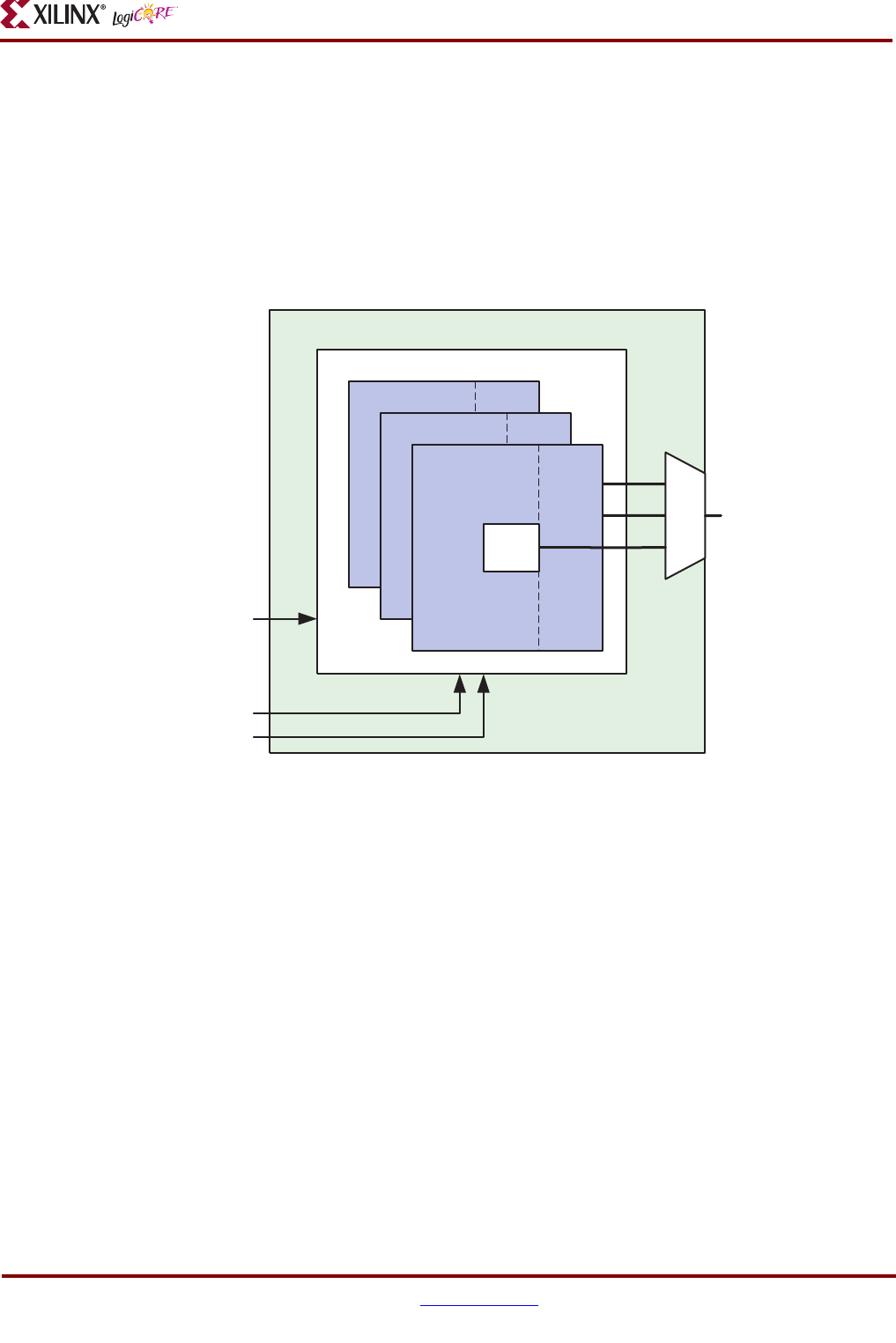
Registers at the output of the block RAM primitives reduce the impact of the clock to out delay of the
primitives. Registers at the output of the core isolate the delay from the block RAMs through the output
multiplexers. Note that each optional register stage used adds an additional clock cycle of latency to the
read operation.
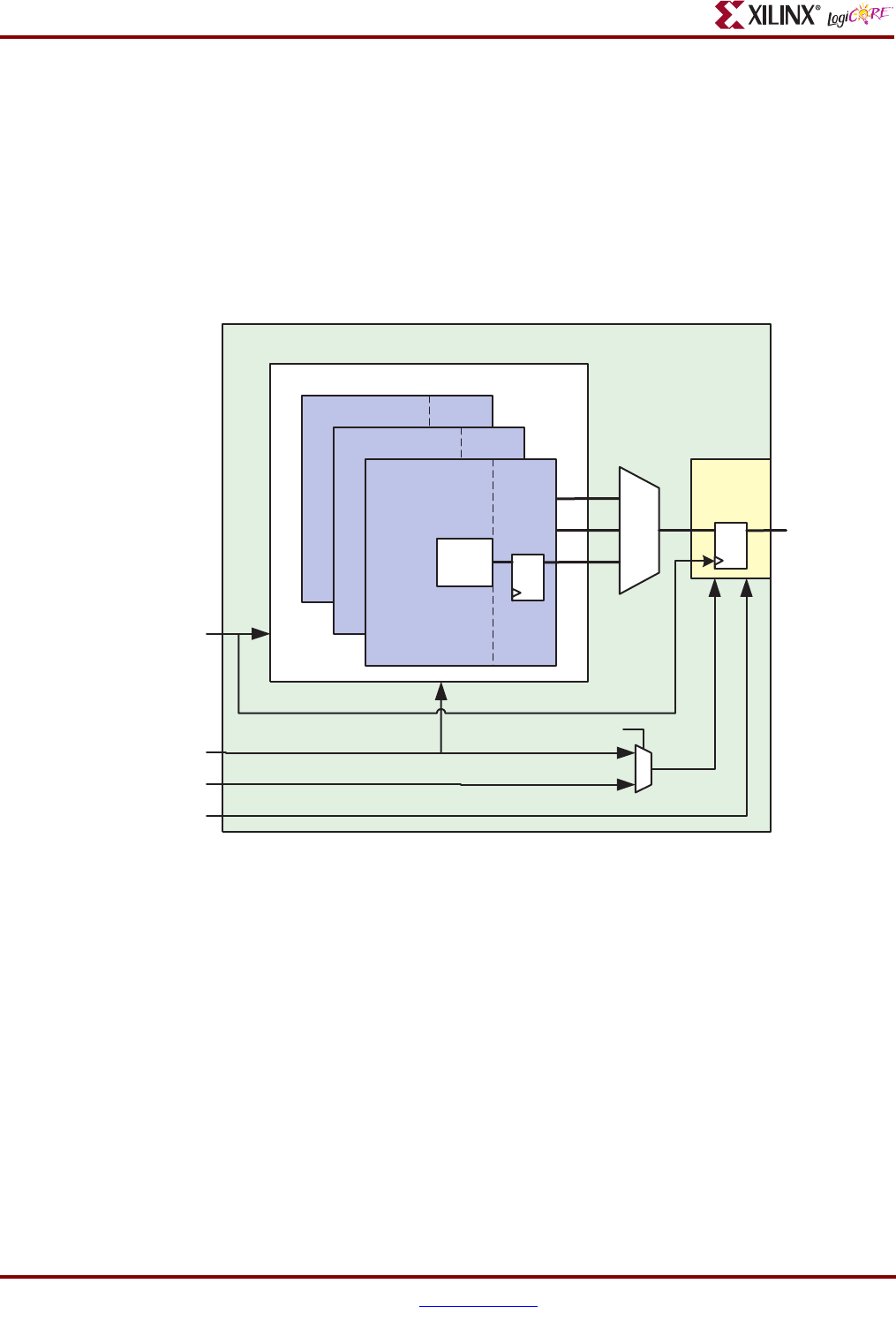
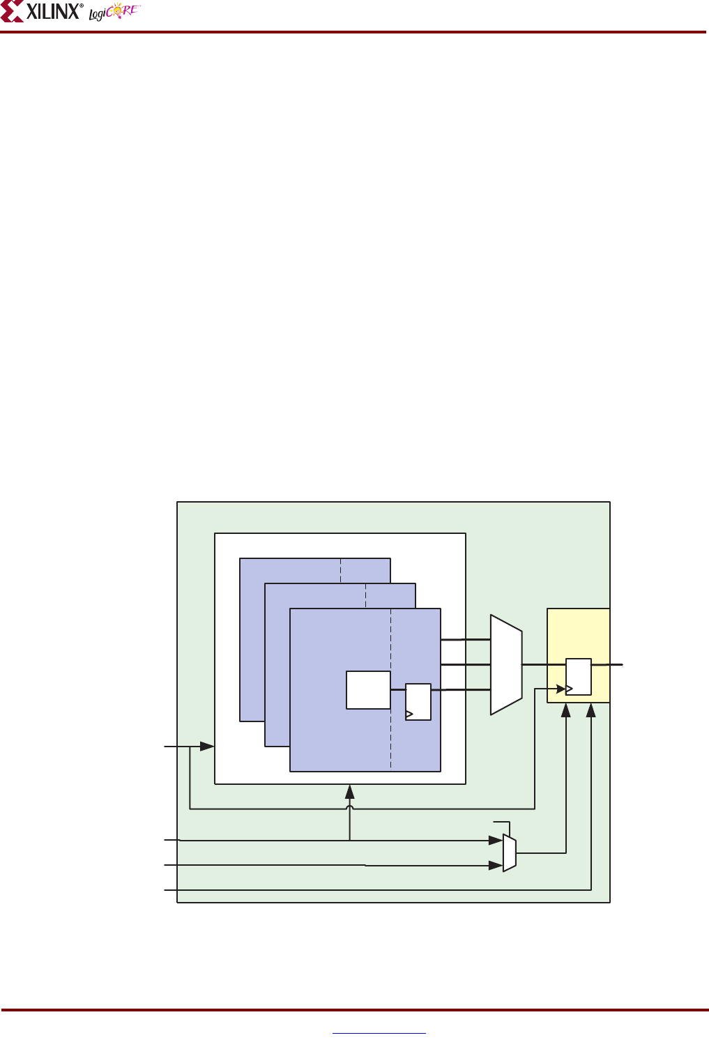
For Virtex-4 FPGAs, the primitive output register stage may be implemented using the Virtex-4 embed-
ded block RAM registers (requiring no further FPGA resources). All other register stages are imple-
mented in FPGA fabric. Figure 19 shows an example of a Virtex-4 based memory that has been
configured using both output register stages.
For a complete description of the output options supported, see it.
Optional Register Clock Enable Pins
The optional output registers are enabled by the EN signal by default. However, the optional register
clock enable pins (
REGCEA and REGCEB) allow the user to control the clock enable pin for the last reg-
ister in the memory output block.
Thus, the data output from the core can be controlled independent of the flow of data through the rest
of the core. When using the
REGCE pin, the last output register operates independently of the EN sig-
nal. For a complete description of the output options supported, see "Output Register Configurations"
on page 37.
Figure Top x-ref 16
Figure 19: Virtex-4 Block Memory Generated With Both Embedded and Core Output Registers Enabled
Block Memory Generator Core
Utilized Block RAM Primitives
Block RAM
Embedded
Output
Registers
Latches
Block RAM
Embedded
Output
Registers
Latches
Core
Output
Registers
EN
HAS_REGCE_PIN
REGCE
0
1
MUX
CLK
SSR
DOUT
Block RAM
Embedded
Output
Registers
Latches
Block Memory Generator v1.1
DS512 January 18, 2006 www.xilinx.com 17
Product Specification
Optional Synchronous Set/Reset Pins
The synchronous set/reset pins (SSRA and SSRB) control the reset operation of the last register in the
output stage. For memories with no output registers, the reset pins control the memory output latches.
When
SSR and EN are asserted on a given port, the data on the output of that port is driven to the reset
value defined in the CORE Generator GUI.
For Virtex-4 FPGAs, if the option to use the synchronous set/reset pin is selected in conjunction with
memory primitive registers and without core output registers, then the Virtex-4 embedded block RAM
registers may not be utilized. For more information, refer to "Output Register Configurations" on
page 37.
Memory Output Flow Control Examples
The combination of the enable (EN), reset (SSR), and register enable (REGCE) pins allow a wide range
of data flows in the output stage. Figure 20 and Figure 21 are examples on how this can be accom-
plished. Keep in mind that the
SSR and REGCE pins apply only to the last register stage.
Figure 20 depicts how
SSR can be used to control the data output to allow only intended data through.
Assume that both output registers are used, the port A reset value is 0xFFFF, and that
EN and REGCE
are always asserted. The data on the block RAM memory latch is labeled LATCH, while the output of
the block RAM embedded register is labeled REG1. The output of the last register is the output of the
core,
DOUT.
Figure 21 depicts how
REGCE can be used to latch the data output to allow only intended data through.
Assume that only the memory primitive registers are used, and that
EN is always asserted and SSR is
Figure Top x-ref 17
Figure 20: Flow Control Using SSR
REG1
CLKA
ADDRA[7:0]
AA BB CC
data(AA) data(BB)
SSR
LATCH
data(AA) data(BB) data(CC)
DOUT
data(AA) data(BB)
DD
FFFFFFFF
data(CC)
data(DD)
data(CC) FFFF
data(DD)
Block Memory Generator v1.1
18 www.xilinx.com DS512 January 18, 2006
Product Specification
always deasserted. The data on the block RAM memory latch is labeled latch, while the output of the
last register, the block RAM embedded register, is the core output,
DOUT.
Simulation Models
The Block Memory Generator core provides two types of functional simulation models to its users:
• Behavioral Simulation Models (VHDL and Verilog)
• Structural/Unisim based Simulation Models (VHDL and Verilog)
The behavioral simulation models is a simplified model of the core while the structural (unisim) based
simulation models is an accurate modeling of the internals of the core. The behavioral simulation mod-
els is written purely in RTL and simulates faster than the structural based simulation models and is
ideal for debugging. Moreover, the memory is modeled in a 2-dimensional array which makes it easier
to probe contents of the memory.
The structural simulation model uses primitive instantiations to more accurately model the behavior of
the core. Collision detection and 'X' generation are better modeled using the structural simulation
model. However, simulation time is longer and debug may be more difficult.
The “Simulation Files” options in the CORE Generator Project Options determines which type of func-
tional simulation models are generated.
Table 2 lists the differences between the two functional simulation models:
Figure Top x-ref 18
Figure 21: Flow Control Using REGCE
Table 2: Differences Between Two Simulation Models
Behavioral Models
Structural (Unisim) based
Models
When core output is undefined. Will never generate ‘X’. Will generate ‘X’ to match core.
Out-of-range address access
Optionally flags a warning
message.
Will generate ‘X’.
Collision behavior
Will not generate ‘X’ on output and
flag a warning message.
Will generate ‘X’ to match core.
Byte-write collision behavior Will flag all byte-write collisions.
Will not flag collisions if byte-writes
do not overlap.
CLKA
ADDRA[7:0]
AA BB CC
REGCE
LATCH
data(AA) data(BB) data(CC)
DOUT
data(AA) data(BB)
DD
data(DD)
data(CC) data(DD)
Block Memory Generator v1.1
DS512 January 18, 2006 www.xilinx.com 19
Product Specification
Signal List
Table 3 provides a description of the Block Memory Generator core signals. The widths of the data ports
(
DINA, DOUTA, DINB, and DOUTB) are selected by the user in the CORE Generator GUI. The address
port (
ADDRA and ADDRB) widths are determined by the memory depth with respect to each port, as
selected by the user in the GUI. The write enable ports (
WEA and WEB) are busses of width 1 when
byte-writes are disabled. When byte-writes are enabled,
WEA and WEB widths depend on the byte size
and write data widths selected in the GUI.
Table 3: Core Signal Pinout
Name Direction Description
CLKA Input
Port A clock: Port A operations are synchronous to this clock. For synchronous
operation, this must be driven by the same signal as CLKB.
ADDRA Input
Port A address: Addresses the memory space for Port A read and write
operations. Available in all configurations.
DINA Input
Port A Data Input: Data input to be written into the memory via Port A. Available
in all RAM configurations.
DOUTA Output
Port A Data Output: Data output from read operations via Port A. Available in
all configurations except simple dual-port RAM.
ENA Input
Port A Clock Enable: Enables read, write, and reset operations via Port A.
Optional in all configurations.
WEA Input
Port A Write Enable: Enables write operations via Port A. Available in all RAM
configurations.
SSRA Input
Port A Synchronous Set/Reset: Resets the Port A memory output latch or
output register. Optional in all configurations.
REGCEA Input
Port A Register Enable: Enables the last output register. Optional in all
configurations with output registers.
CLKB Input
Port B Clock: Port B operations are synchronous to this clock. Available in
dual-port configurations. For synchronous operation, this must be driven by the
same signal as CLKA.
ADDRB Input
Port B address: Addresses the memory space for Port B read and write
operations. Available in dual-port configurations.
DINB Input
Port B Data Input: Data input to be written into the memory via Port B. Available
in true dual-port RAM configurations.
DOUTB Output
Port B Data Output: Data output from read operations via Port B. Available in
dual-port configurations.
ENB Input
Port B Clock Enable: Enables read, write, and reset operations via Port B.
Optional in dual-port configurations.
WEB Input
Port B Write Enable: Enables write operations via Port B. Available in dual-port
RAM configurations.
SSRB Input
Port B Synchronous Set/Reset: Resets the Port B memory output latch or
output register. Optional in dual-port configurations.
REGCEB Input
Port B Register Enable: Enables the last output register. Optional in dual-port
configurations with output registers.

Block Memory Generator v1.1
20 www.xilinx.com DS512 January 18, 2006
Product Specification
Generating the Core
The Block Memory Generator can be found in the CORE Generator GUI View by Function pane: Under
Memories & Storage Elements > RAMs & ROMs. This section describes the options available in the
Block Memory Generator GUI.
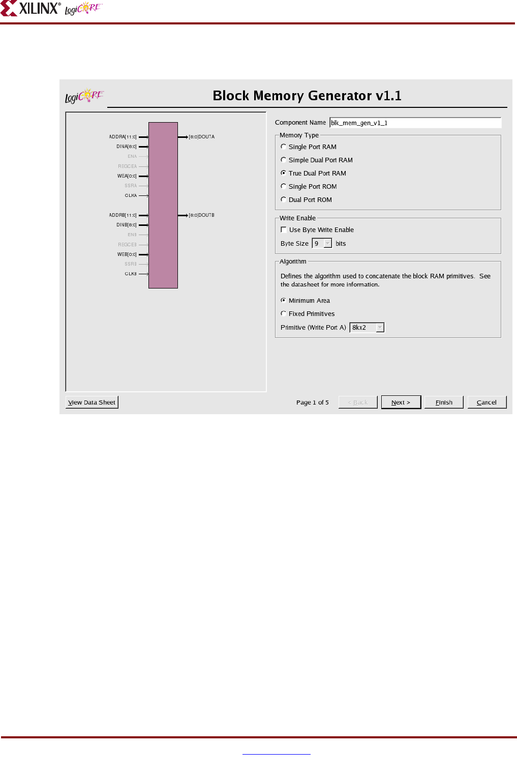
CORE Generator Parameter Screens
The Block Memory Generator GUI includes five screens:
• Block Memory Generator Main Screen
• Port A Options Screen
• Port B Options Screen
• Output Registers and Memory Initialization Screen
• Simulation Model Options and Information Screen
In addition, all the screens share common tabs and buttons to provide information about the core and
to navigate the Block Memory Generator GUI.
Block Memory Generator v1.1
DS512 January 18, 2006 www.xilinx.com 21
Product Specification
Block Memory Generator Main Screen
Component Name
The base name of the output files generated for the core. Names must begin with a letter and be com-
posed of any of the following characters: a to z, 0 to 9, and “_”. Names can not be Verilog or VHDL
reserved words.
Memory Type
Select the type of memory to be generated.
•Single-port RAM
• Simple dual-port RAM
• True dual-port RAM
•Single-port ROM
• Dual-port ROM configurations.
Write Enable
When targeting Virtex-4, select whether to use the byte-write enable feature. Byte size is 9 bits, though
it may be optional in future versions.
Figure Top x-ref 19
Figure 22: Block Memory Generator Main Screen
Block Memory Generator v1.1
22 www.xilinx.com DS512 January 18, 2006
Product Specification
Algorithm
Select the algorithm used to implement the memory.
• Minimum Area Algorithm: Generates a core using the least number of primitives.
• Selectable Primitive Algorithm: Generates a core that concatenates a single primitive type to
implement the memory. Choose which primitive type to use in the drop down box.
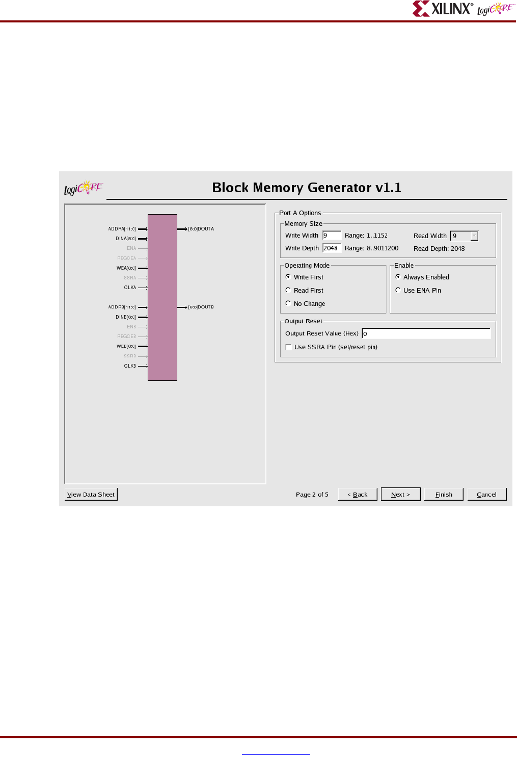
Port A Options Screen
Memory Size (Port A)
Specify the port A write width and depth. Select the port A read width from the drop-down menu of
valid choices. The read depth is calculated automatically.
Operating Mode (Port A)
Specify the port A operating mode.
•READ_FIRST
•WRITE_FIRST
•NO_CHANGE
Figure Top x-ref 20
Figure 23: Port A Options
Block Memory Generator v1.1
DS512 January 18, 2006 www.xilinx.com 23
Product Specification
Enable (Port A)
Select the enable type:
• Always enabled (no
ENA pin available)
•Use
ENA pin
Output Reset (Port A)
Specify the reset value of the memory output latch and output registers. These values are with respect
to the read port widths. Choose whether a set/reset pin (
SSRA) is needed.
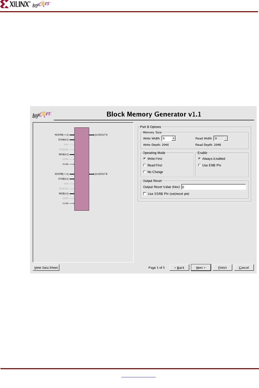
Port B Options Screen
Memory Size (Port B)
Select the port B write and read widths from the drop-down menu of valid choices. The read depth is
calculated automatically.
Operating Mode (Port B)
Specify the port B write mode.
•READ_FIRST
•WRITE_FIRST
Figure Top x-ref 21
Figure 24: Port B Options
Block Memory Generator v1.1
24 www.xilinx.com DS512 January 18, 2006
Product Specification
•NO_CHANGE
Enable (Port B)
Select the enable type:
• Always enabled (no
ENB pin available)
•Use
ENB pin
Output Reset (Port B)
Specify the reset value of the memory output latch and output registers. These values are with respect
to the read port widths. Choose whether a set/reset pin (
SSRB) is needed.
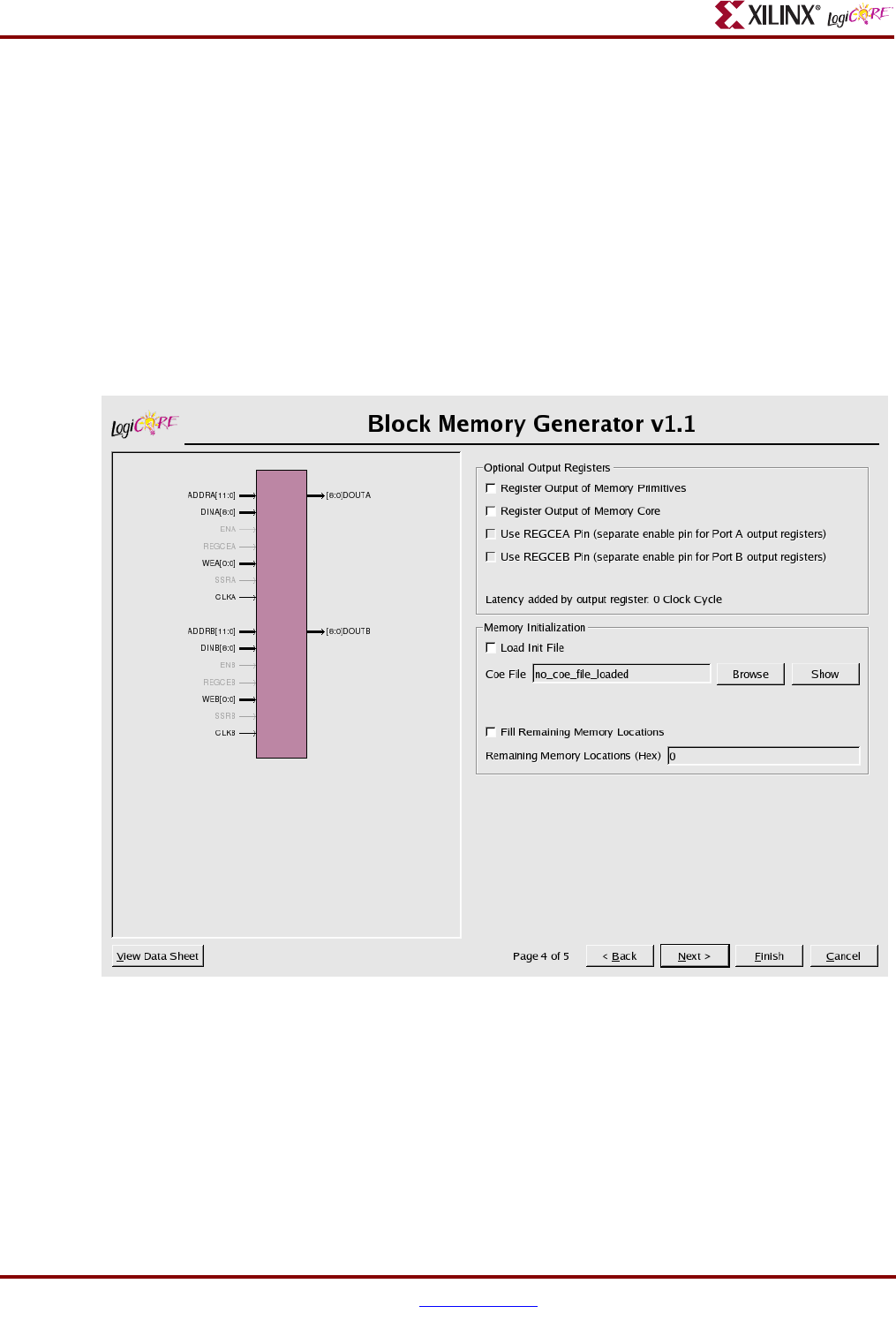
Output Registers and Memory Initialization Screen
Optional Output Registers
Select which output register stages to include:
• Register Output of Memory Primitives. Select to insert output register after the memory
primitives. When targeting Virtex-4 FPGAs, the embedded output registers in the block RAM
primitives will be used if the user chooses to registers the output of the memory primitives. For
other architectures, the registers in the FPGA slices will be used.
• Register Output of Memory Core. Select to insert register output of the memory core. The registers
Figure Top x-ref 22
Figure 25: Output Registers and Memory Initialization Screen
Block Memory Generator v1.1
DS512 January 18, 2006 www.xilinx.com 25
Product Specification
in the FPGA slices will be used.
Select whether to have separate enable pins for the last register stage if output registers are selected.
Memory Initialization
Select whether to initialize the memory contents using a COE file, and whether to initialize the remain-
ing memory contents with a default value. When using asymmetric port widths or data widths, the
COE file and the default value are with respect to the port A write width.
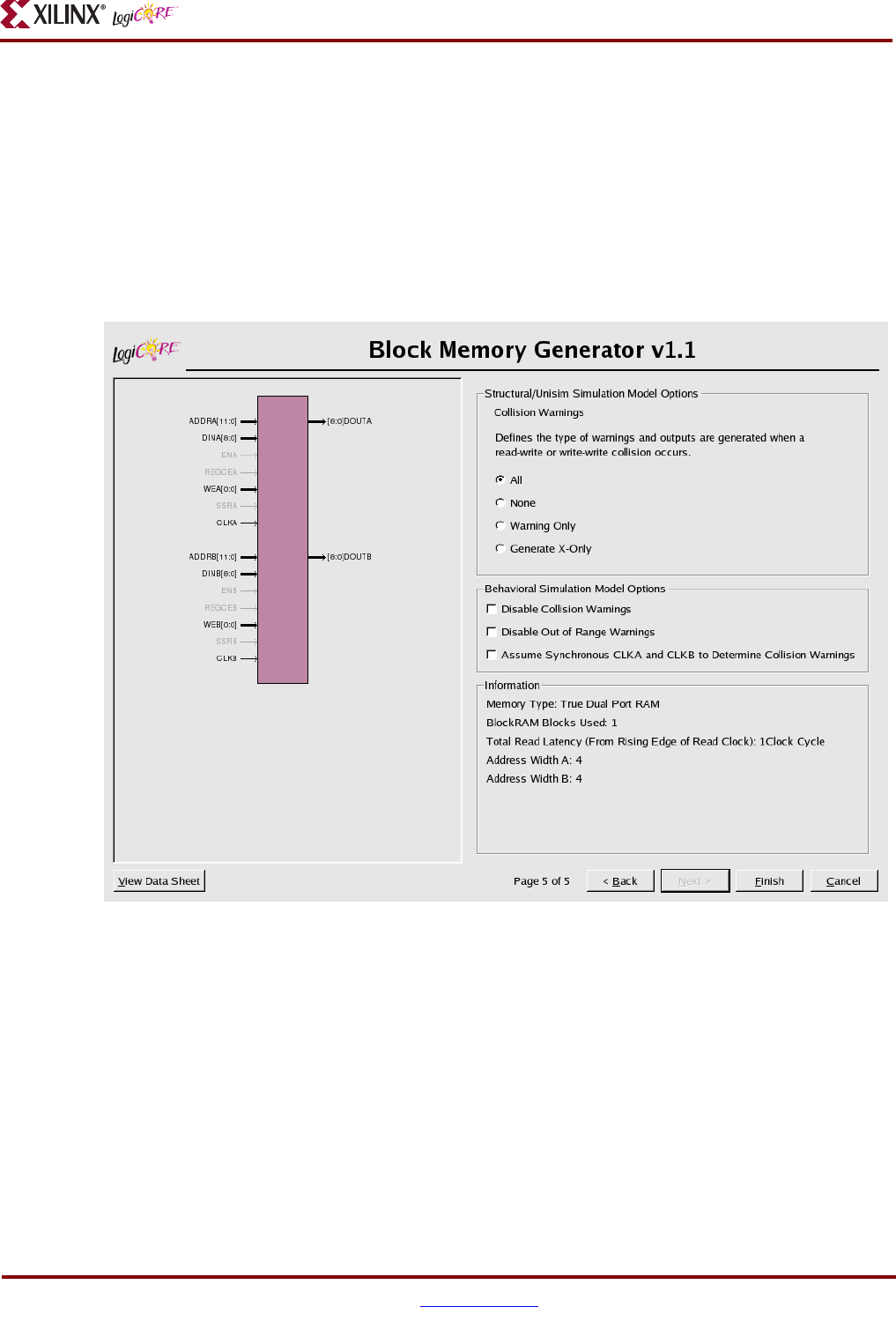
Simulation Model Options and Information Screen
Structural/UNISIM Simulation Model Options
Select the type of warning messages and outputs generated by the structural simulation model in the
event of collisions.
Behavioral Simulation Model Options
Select the type of warning messages generated by the behavioral simulation model. Select whether the
model should assume synchronous clocks for collision warnings.
Information Panel
This pane displays an informational summary of the selected core options.
Figure Top x-ref 23
Figure 26: Simulation Model Options and Information Screen

Block Memory Generator v1.1
26 www.xilinx.com DS512 January 18, 2006
Product Specification
Specifying Initial Memory Contents
The Block Memory Generator core supports memory initialization using a memory coefficient (COE)
file, the default data option in the CORE Generator GUI, or a combination of both.
The COE file can specify the initial contents of each memory location, while default data specifies the
contents of all memory locations. When used in tandem, the COE file can specify a portion of the mem-
ory space, while default data fills the rest the remaining memory space. COE files and default data shall
be formatted with respect to the port A write width (or port A read width for ROM’s).
A COE a text file which specifies two parameters:
• memory_initialization_radix: The radix of the values in the memory_initialization_vector. Valid
choices are 2, 10, or 16.
• memory_initialization_vector: Defines the contents of each memory element. Each value is
LSB-justified, separated by a space, and assumed to be in the radix defined by
memory_initialization_radix.
The following is an example COE file. Note that semi-colon is the end of line character.
; Sample initialization file for a
; 32-bit wide by 16 deep RAM
memory_initialization_radix = 16;
memory_initialization_vector =
0 1 2 3 4 5 6 7
8 9 A B C D E F;
Verification
The Block Memory Generator core and the simulation models delivered with it are rigorously verified
using advanced verification techniques, including a constrained-random configuration generator and
a cycle-accurate bus functional model.
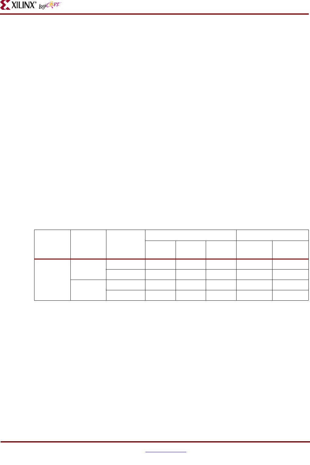
Resource Utilization and Performance
The resource utilization and performance of the Block Memory Generator core is highly dependent on
user selections, such as algorithm, optional output registers, and memory size.
Block RAM Usage
When using the fixed primitive algorithm, the number of block RAM primitives used is equal to the
width ratio (rounded up) multiplied by the depth ratio (rounded up), where the width ratio is the
width of the memory divided by the width of the selected primitive, and the depth ratio is the depth of
the memory divided by the depth of the primitive selected.
When using the minimum area algorithm, it is not as easy to determine the exact block RAM count.
This is because the actual algorithm performs complex manipulations to produce an optimal solution.
The optimistic estimate is total memory bits divided by 18k (the total number of bits per primitive)
rounded up. Given that the algorithm packs block RAM’s very efficiently, this estimate is often very
accurate for most memories.
LUT Utilization and Performance
The LUT utilization and performance of the core are directly related to the arrangement of primitives
and the selection of output registers. Particularly, the number of primitives cascaded in depth to imple-
Block Memory Generator v1.1
DS512 January 18, 2006 www.xilinx.com 27
Product Specification
ment a memory determines the size of the output multiplexer and the size of the input decoder, which
are implemented in the FPGA fabric.
It should be noted that while the minimum area algorithm’s primary goal is to use the minimum num-
ber of block RAM primitives, it has a secondary goal of maximizing performance – as long as block
RAM usage does not increase.
Resource Utilization and Performance Examples
The following tables provide examples of actual resource utilization and performance for Block Mem-
ory Generator implementations. Each section highlights the effects of a specific feature on resource uti-
lization and performance.
Benchmarks were performed targeting a Virtex-II Pro FPGA in the -5 speed grade (2vp30-ff1152-5) and
a Virtex-4 FPGA in the -10 speed grade (4vlx60-ff1148-10). Better performance may be possible with
higher speed grades.
In the benchmark designs below, the core was encased in a wrapper with input and output registers to
remove the effects of IO delays from the results; performance may vary depending on the user design.
The minimum area algorithm was used unless otherwise noted. The examples below highlight the use
of embedded registers in Virtex-4 and the subsequent significant performance improvement.
Single Primitive
The Block Memory Generator does not add additional logic if the memory can be implemented in a sin-
gle Block RAM primitive. Table 4 shows performance data for single-primitive memories.
Table 4: Single Primitive Examples
Memory
Type
Options
Width x
Depth
Resource Utilization Performance
Block
RAMs
LUTs FFs
Virtex-II
Pro
Virtex-4
True
Dual-Port
RAM
36x512 1 0 0 331 307
9x2k 1 0 0 350 351
1
36x512 1 0 0 N/A 365
9x2k 1 0 0 N/A 400
Options
1. Virtex-4 embedded output registers
Block Memory Generator v1.1
28 www.xilinx.com DS512 January 18, 2006
Product Specification
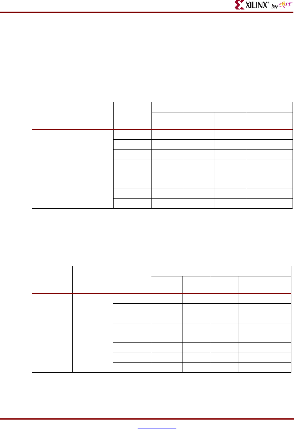
Output Registers
The Block Memory Generator optional output registers increase the performance of memories by iso-
lating the Block RAM primitive clock-to-out delays and the data output multiplexer delays.
The output registers are only implemented for output ports. For this reason, when output registers are
used, a single port RAM requires fewer resources than a true dual port RAM. Note that the effects of the
core output registers are not fully illustrated due to the simple register wrapper used. In a full-scale
user design, core output registers may improve performance notably.
In Virtex-4 architectures, the embedded Block RAM may be utilized, reducing the FPGA fabric
resources required to create the registers.
Table 5: Virtex-II Pro Output Register Examples
Memory
Type
Width x
Depth
Options
Virtex-II Pro
Block
RAMs
FFs LUTs
Performance
(MHz)
True Dual-Port
RAM
17x5k
5 6 42 290
1 5 98 110 288
2 5 40 42 291
1,2 5 134 76 344
Single-Port
RAM
17x5k
5 3 21 297
1 5 49 55 312
2 5 20 21 299
1,2 5 67 38 350
Options
1. Primitive output registers
2. Core output registers
Table 6: Virtex-4 Output Register Examples
Memory
Type
Width x
Depth
Options
Virtex-4
Block
RAMs
FFs LUTs
Performance
(MHz)
True Dual-Port
RAM
17x5k
5642 249
1 5 12 42 327
2 5 40 42 253
1,2 5 52 42 370
Single-Port
RAM
17x5k
5321 263
15621 375
2 5 20 21 263
1,2 5 26 21 382
Options
1. Embedded primitive output registers
2. Core output registers
Block Memory Generator v1.1
DS512 January 18, 2006 www.xilinx.com 29
Product Specification
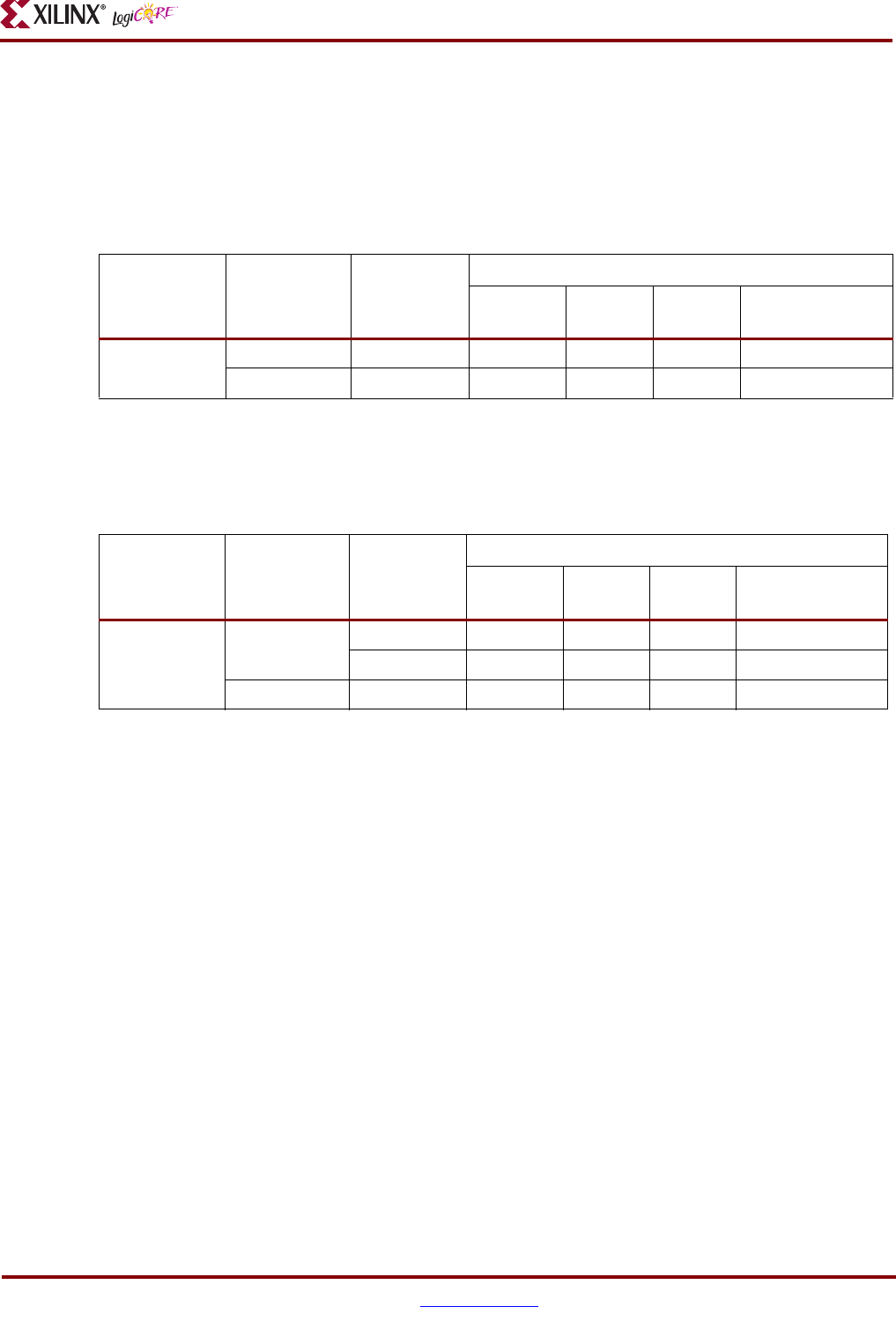
Aspect Ratios
The Block Memory Generator selectable port and data width aspect ratios may increase Block RAM
usage and affect performance, because aspect ratios limit the primitive types available to the algorithm,
which can reduce packing efficiency. Large aspect ratios, such as 1:32, have a greater impact than small
aspect ratios. Note that width and depth are reported with respect to the port A write interface.
Table 7: Virtex-II Pro Aspect Ratio Examples
Memory
Type
Width x
Depth
Options
Virtex-II Pro
Block
RAMs
FFs LUTs
Performance
(MHz)
True Dual-Port
RAM
17x5k 1 5 6 42 290
136x640 2 9 0 0 259
Options
1. Port aspect ratio = 1:1
2. Port aspect ratio = 1:8 (A port is 136x640; B port is 17x5k)
Table 8: Virtex-4 Aspect Ratio Examples
Memory
Type
Width x
Depth
Options
Virtex-4
Block
RAMs
FFs LUTs
Performance
(MHz)
Single-Port
RAM
17x5k
15321263
2900 301
136x640 3 9 0 0 319
Options
1. Data width aspect ratio = 1:1
2. Data width aspect ratio = 1:8 (read port is 136x640, write port is 17x5k)
3. Data width aspect ratio = 8:1 (read port is 17x5k, write port is 136x640)
Block Memory Generator v1.1
30 www.xilinx.com DS512 January 18, 2006
Product Specification
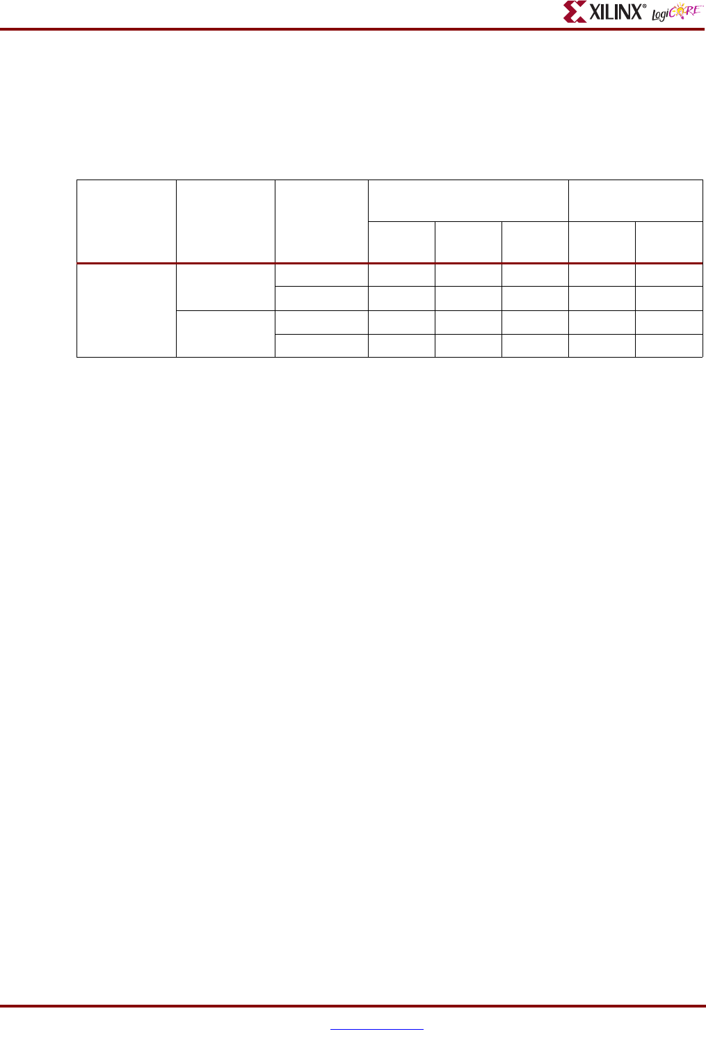
Algorithm
The differences between the minimum area algorithm and the selectable primitive algorithm are dis-
cussed in detail in "Selectable Memory Algorithm" on page 2. Table 9 shows examples of the resource
utilization and the performance difference between them for two selected configurations.
Table 9: Memory Algorithm Examples
Memory
Type
Width x
Depth
Options
Resource Utilization
Performance
(MHz)
Block
RAMs
FFs LUTs
Virtex-II
Pro
Virtex-4
Single-Port
RAM
17x5k
1 5 3 21 297 263
2 5 3 56 292 247
36x4k
1 8 1 38 285 291
3 8 4 152 252 217
Options
1. Minimum area algorithm
2. Selectable Primitive Algorithm using 18x1k Block RAMs
3. Selectable Primitive Algorithm using 36x512 Block RAMs
Block Memory Generator v1.1
DS512 January 18, 2006 www.xilinx.com 31
Product Specification
Supplemental Information
The following sections provide additional information about working with the Block Memory Genera-
tor core.
• Interfacing with Older Memory Cores. Defines the differences between older memory cores and the
Block Memory Generator core.
• SIM Parameters. Defines the SIM parameters used to specify the core configuration.
• Output Register Configurations. Provides information optional output registers used to improve
core performance.
Interfacing with Older Memory Cores
This section describes the differences between the LogiCORE Single and Dual Port Block Memory cores
and the Block Memory Generator. The new Block Memory Generator is not backward compatible with
the Single and Dual Port Block Memory core in several aspects:
• Single Port Block Memory core and the Block Memory Generator do not have the same port names
for a single-port memory configuration
• Dual Port Block Memory core and the Block Memory Generator do not have the same reset pin
name
• XCO files for the previous memory cores are NOT compatible with the Block Memory Generator
• Pin polarity, handshaking, and input register features supported by the previous memory cores are
not supported in the Block Memory Generator
• The behavior of set/reset pin (
SSR) and the enable pin (EN) in the Block Memory Generator will
differ from previous cores when using optional output registers
Port Memory Pin Names
In the Block Memory Generator, the port names have been changed to reflect the actual ports on the
block RAM primitives. Table 10 and Table 11 reflect the changes in port names.
Table 10: Port Name Changes from Single Port Block Memory Core
Single Port Block Memory v6.2
(Old core)
Block Memory Generator v1.1
(New Core, Single Port Configuration)
DIN DINA
ADDR ADDRA
EN ENA
WE WEA
SINIT SSRA
CLK CLKA
DOUT DOUTA
ND
Not supported
RFD
Not supported
RDY
Not supported
Block Memory Generator v1.1
32 www.xilinx.com DS512 January 18, 2006
Product Specification
Obsolete Features
Minimum Parameterizable Depth
The minimum depth for the previous cores is 2. The Block Memory Generator core has a minimum
depth of 8.
Pin Polarity 0ption
The Block Memory Generator does not support pin polarity options on the clock, enable, write enable
and set/reset input pins. When active low signaling is desired, users can invert the signals prior to the
input of the core.
Handshaking Pins
The Block Memory Generator does not support handshaking pins:
ND[A|B], RFD[A|B] and
RDY[A|B].
Input Registers
The Block Memory Generator does not support input registers on port
DIN, ADDR, and WE prior to
accessing the memory primitives.
Modified Behaviors
Enable Pin
Table 12 illustrates the difference in enable behavior between the previous cores and the Block Memory
Generator.
Table 11: Port Name Changes from Dual Port Block Memory Core
Dual Port Block Memory v6.2
(Old core)
Block Memory Generator v1.1
(New Core, Single Port Configuration)
SINITA SSRA
SINITB SSRB
ND [A|B]
Not supported
RFD [A|B]
Not supported
RDY [A|B]
Not supported
Table 12: Old and New Core Differences
Single (or Dual) Port Block Memory
v6.2
Block Memory Generator v1.1
1
Enable signal is pipelined and each pipeline
register enables the registers or memories in
that pipe stage
Enable signal in NOT pipelined and is tied directly to
the enables for all registers and memories
2
Single enable pin that controls the enables of
all registers and memories
Two optional enable pins provided:
•
REGCE pin that only controls the enables of
the registers in the last output stage
• EN pin that controls the enables of all other
registers and memory

Block Memory Generator v1.1
DS512 January 18, 2006 www.xilinx.com 33
Product Specification
Synchronous Reset Pin
In the previous memory cores, the synchronous reset (
SINIT pin) initializes all memory latches and
output registers. In the Block Memory Generator, the synchronous set/reset (
SSR pin) only resets the
registers in the last output stage. When there are no output register stages present, it will initialize the
memory latches.
Block Memory Generator v1.1
34 www.xilinx.com DS512 January 18, 2006
Product Specification
SIM Parameters
Table 13 defines the SIM parameters used to specify the configuration of the core. These parameters are
only used to manually instantiate the core in HDL, calling the CORE Generator dynamically. This
parameter list does not apply to users that generate the core using the CORE Generator GUI.
Table 13: SIM Parameters
SIM Parameter Type Range Description
1 C_FAMILY String
Spartan-3, Spartan-3E,
Virtex-II, Virtex-II Pro, Virtex-4,
Target device family
2 C_MEM_TYPE Integer
0: Single Port RAM
1: Simple Dual Port RAM
2: True Dual Port RAM
3: Single Port ROM
4: Dual Port RAM
Type of memory
3 C_ALOGRITHM
0 (selectable primitive),
1 (minimum area)
Type of algorithm
4 C_PRIM_TYPE Integer
0 (1-bit wide)
1 (2-bit wide)
2 (4-bit wide)
3 (9-bit wide)
4 (18-bit wide)
5 (36-bit wide)
6 (72-bit wide, single-port only)
If selectable primitive
algorithm is chosen,
defines which type of
primitive to use to build
memory
5 C_BYTE_SIZE Integer 8, 9
Defines size of a byte;
8-bit or 9-bit
6 C_SIM_COLLISION_CHECK String
None, Generate_X, All,
Warnings_only
Defines warning collision
checks in
structural/unisim
simulation model
7 C_COMMON_CLOCK Integer 0, 1
Defines whether to
optimize behavioral
model collision check by
assume clocks are
synchronous
8
C_DISABLE_WARN_BHV_COL
L
Integer 0, 1
Disables the behavioral
model from generating
warnings due to
read-write collisions
9
C_DISABLE_WARN_BHV_RAN
GE
Integer 0, 1
Disables the behavioral
model from generating
warnings due to address
out of range
10 C_LOAD_INIT_FILE Integer 0, 1
Defined whether to load
initialization file
11 C_INIT_FILE_NAME String “…”
Name of initialization file
(MIF format)
12 C_USE_DEFAULT_DATA Integer 0, 1
Defines whether to use
default data for the
memory

Block Memory Generator v1.1
DS512 January 18, 2006 www.xilinx.com 35
Product Specification
13 C_DEFAULT_DATA String “…”
Defines a default data for
the memory
14 C_HAS_MEM_OUTPUT_REGS Integer 0, 1
Defines whether a
register stage is added at
the output of the memory
latch
15 C_HAS_MUX_OUTPUT_REGS Integer 0, 1
Defines whether a
register stage is added at
the output of the memory
core
16 C_WRITE_WIDTHA Integer 1 to 1152
Defines width of write
port A
17 C_READ_WIDTHA Integer 1 to 1152
Defines width of read port
A
18 C_WRITE_DEPTHA Integer 8 to 9011200
Defines depth of write
port A
19 C_READ_DEPTHA Integer 8 to 9011200
Defines depth of read
port A
20 C_ADDRA_WIDTH Integer 3 to 24
Defines the width of
address A
21 C_WRITE_MODEA String
Write_First, Read_first,
No_change
Defines the write mode
for port A
22 C_HAS_ENA Integer 0, 1
Defines whether port A
has an enable pin
23 C_HAS_REGCEA Integer 0, 1
Defines whether port A
has an enable pin for its
output register
24 C_HAS_SSRA Integer 0, 1
Defines whether port A
has an synchronous reset
pin
25 C_SINITA_VAL String “…”
Defines
initialization/power-on
value for port A output
26 C_USE_BYTE_WEA Integer 0, 1
Defines whether
byte-write feature is used
on port A
27 C_WEA_WIDTH Integer 1 to 128
Defines width of
WEA pin
for port A
28 C_WRITE_WIDTHB Integer 1 to 1152
Defines width of write
port B
29 C_READ_WIDTHB Integer 1 to 1152
Defines width of read port
B
30 C_WRITE_DEPTHB Integer 8 to 9011200
Defines depth of write
port B
Table 13: SIM Parameters (Continued)
SIM Parameter Type Range Description
Block Memory Generator v1.1
36 www.xilinx.com DS512 January 18, 2006
Product Specification
31 C_READ_DEPTHB Integer 8 to 9011200
Defines depth of read
port B
32 C_ADDRB_WIDTH Integer 3 to 24
Defines the width of
address B
33 C_WRITE_MODEB String
Write_First, Read_first,
No_change
Defines the write mode
for port B
34 C_HAS_ENB Integer 0, 1
Defines whether port B
has an enable pin
35 C_HAS_REGCEB Integer 0, 1
Defines whether port B
has an enable pin for its
output register
36 C_HAS_SSRB Integer 0, 1
Defines whether port B
has an synchronous reset
pin
37 C_SINITB_VAL String “…”
Defines
initialization/power-on
value for port B output
38 C_USE_BYTE_WEB Integer 0, 1
Defines whether
byte-write feature is used
on port B
39 C_WEB_WIDTH Integer 1 to 128
Defines width of
WEA pin
for port B
Table 13: SIM Parameters (Continued)
SIM Parameter Type Range Description
Block Memory Generator v1.1
DS512 January 18, 2006 www.xilinx.com 37
Product Specification
Output Register Configurations
The Block Memory Generator core allows optional output registers to improve the performance of the
core. Since Virtex-4 block RAM primitives have embedded output registers that the previous architec-
tures did not support, the configurations described below are separated into Virtex-4 and non-Virtex-4
implementations. Note that each optional register used adds an additional clock cycle of latency to the
read operation.
Virtex-4 Output Register Configurations
To tailor the register options, two check boxes are provided in the CORE Generator GUI under the Out-
put Pipelining section. The embedded output registers are enabled when the box labeled “Register out-
put of memory primitive” is checked. Likewise, registers at the output of the core are enabled by checking
the box labeled “Register output of memory core.” Illustrated below are the resulting implementations of
the four permutations supported by these configuration options.
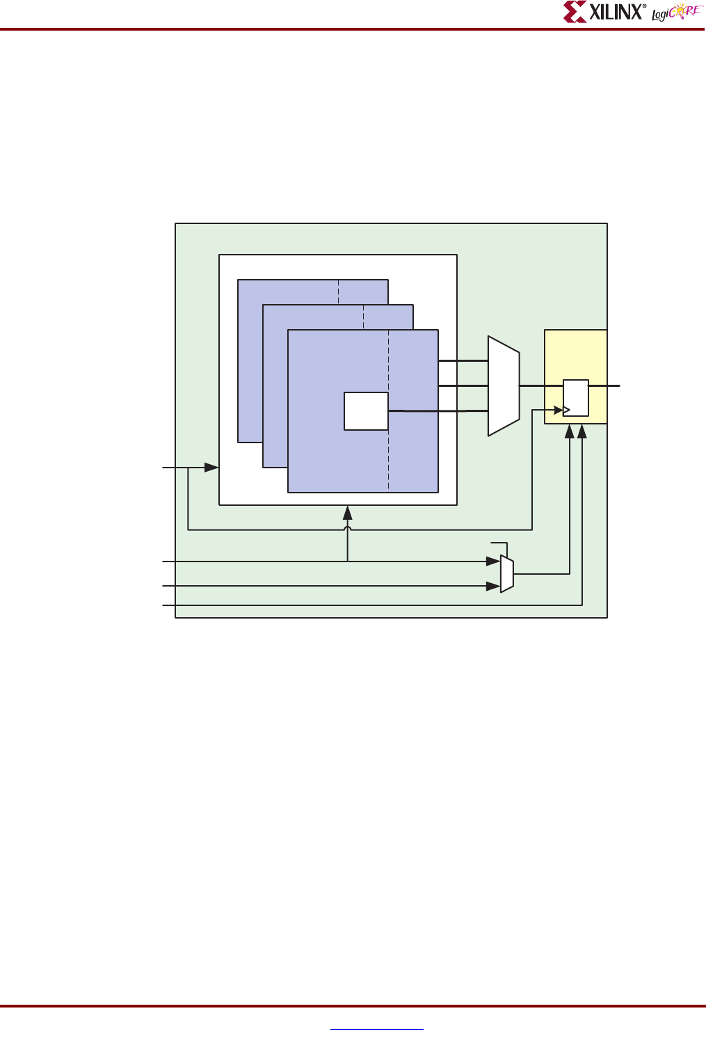
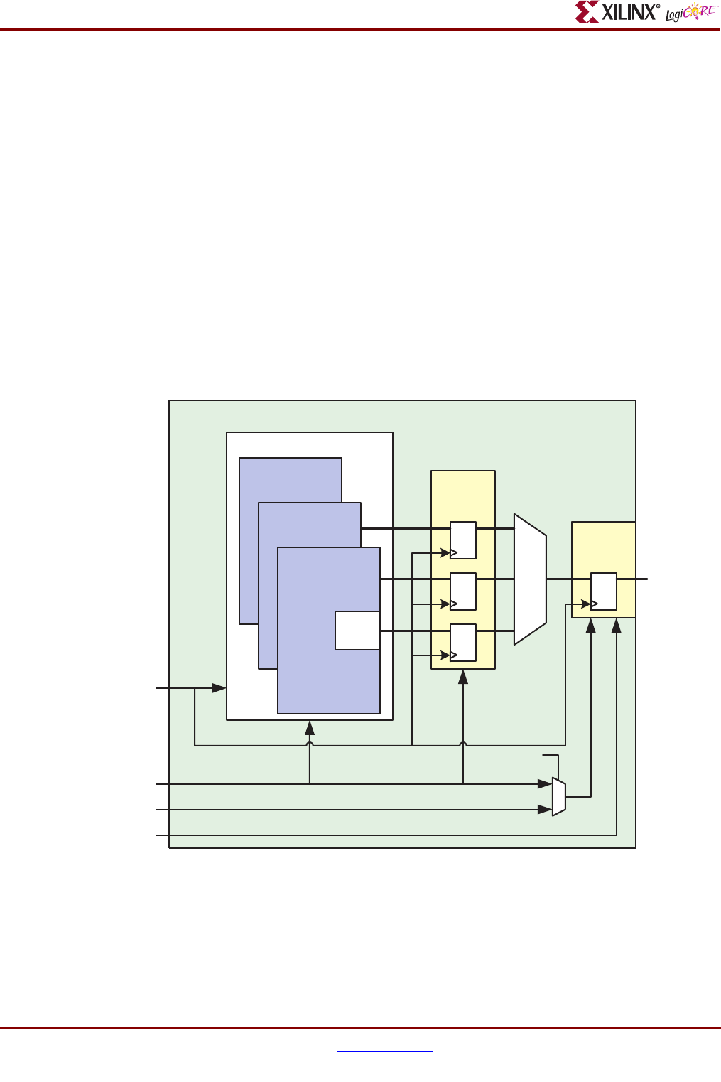
Virtex-4 Memory with Embedded and Core Output Registers
When both options are selected, then a memory core is generated with both the Virtex-4 embedded reg-
isters enabled and a set of registers on the output, as shown in Figure 27. If you are building a large
memory construct, selecting this configuration can provide improved performance.
; Register output of memory primitive
; Register output of memory core
Figure Top x-ref 24
Figure 27: Virtex-4 Block Memory Generated With Both Embedded and Core Output Registers Enabled
Block Memory Generator Core
Utilized Block RAM Primitives
Block RAM
Embedded
Output
Registers
Latches
Block RAM
Embedded
Output
Registers
Latches
Core
Output
Registers
EN
HAS_REGCE_PIN
REGCE
0
1
MUX
CLK
SSR
DOUT
Block RAM
Embedded
Output
Registers
Latches
Block Memory Generator v1.1
38 www.xilinx.com DS512 January 18, 2006
Product Specification
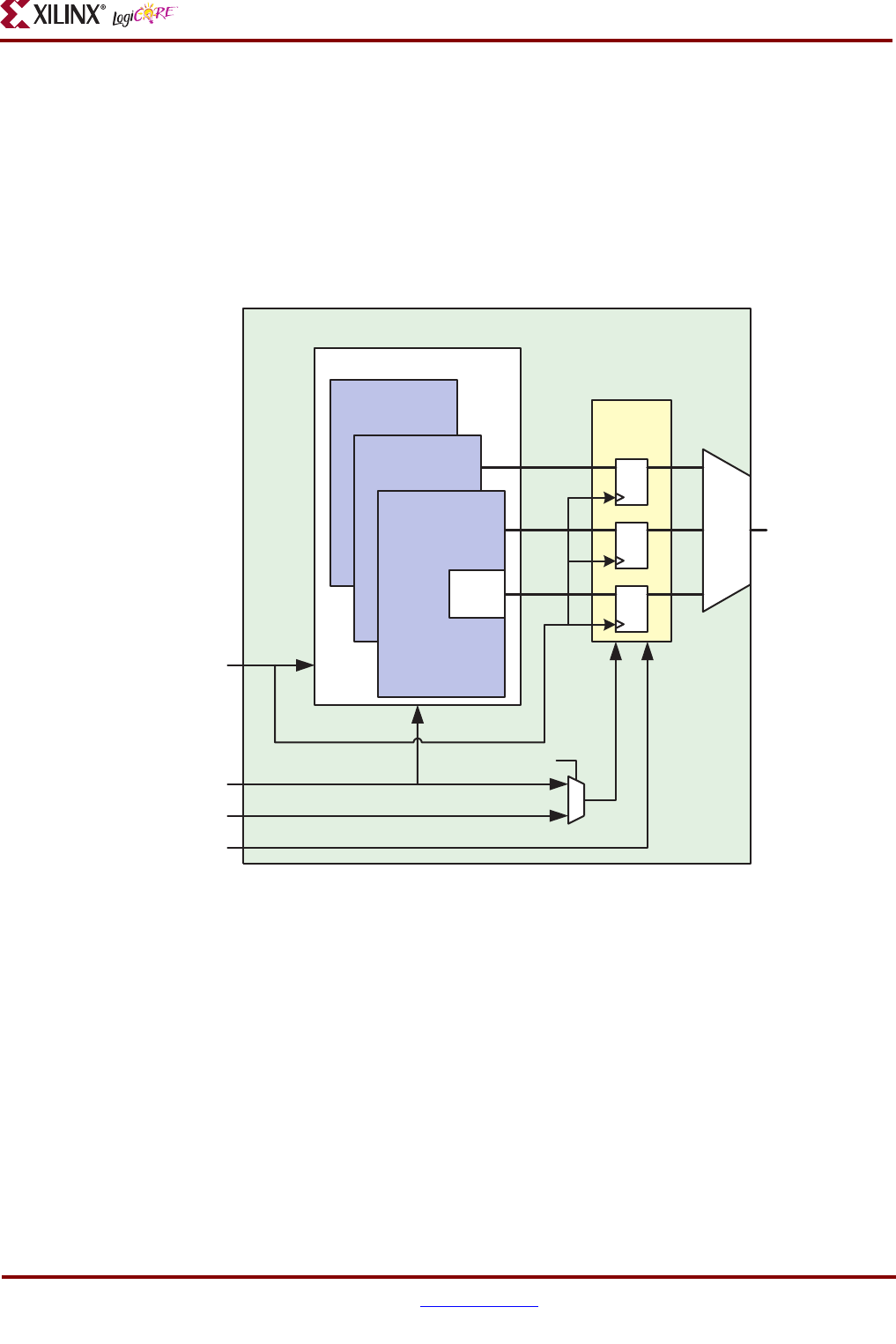
Virtex-4 Memory with Embedded Registers Only
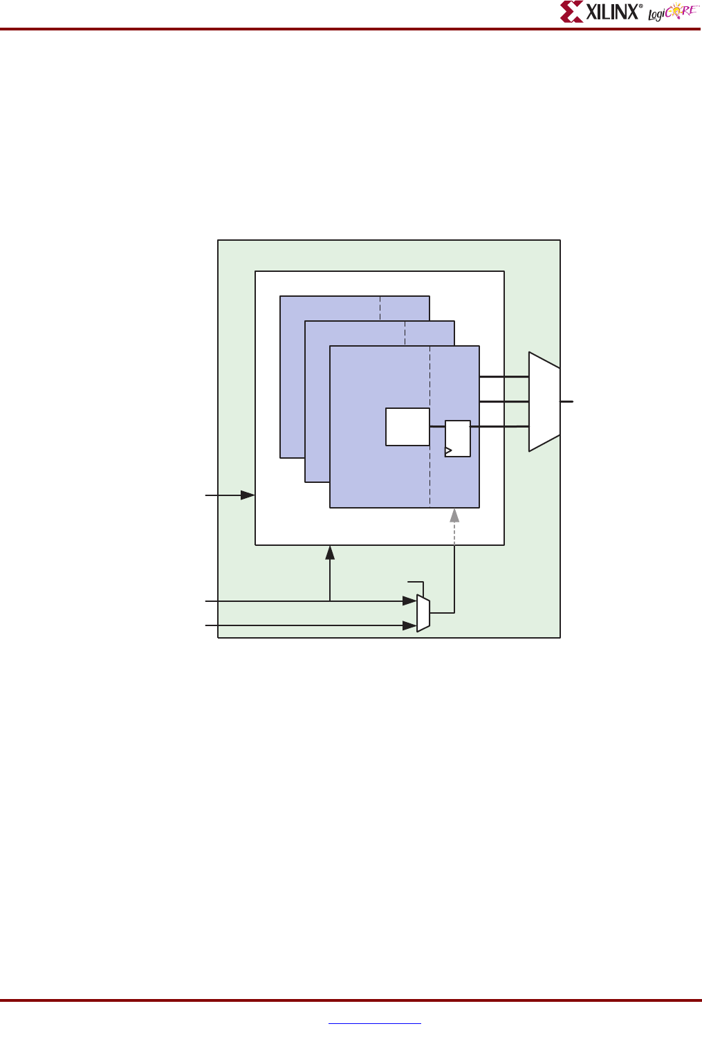
When only the option to use the primitive registers is selected, then a memory core is generated that
registers the output of the block RAM primitives. Note that the output of any multiplexing which may
be required to combine multiple primitives, will be not be registered in this configuration, as shown in
Figure 28.
; Register output of memory primitive
Register output of memory core
Figure Top x-ref 25
Figure 28: Virtex-4 Block Memory Generated With Embedded Registers
Block Memory Generator Core
Utilized Block RAM Primitives
Block RAM
Embedded
Output
Registers
Latches
Block RAM
Embedded
Output
Registers
Latches
EN
HAS_REGCE_PIN
REGCE
0
1
MUX
CLK
DOUT
Block RAM
Embedded
Output
Registers
Latches
Block Memory Generator v1.1
DS512 January 18, 2006 www.xilinx.com 39
Product Specification
If the option to use the synchronous reset pin (SSRA, SSRB) is selected, then the Virtex-4 embedded
block RAM registers can not be utilized. The primitive registers will be built from FPGA fabric as illus-
trated in Figure 29. If an extra cycle of latency is acceptable, then select both register stages as shown
above in Figure 27 to enable the Virtex-4 embedded block RAM registers.
; Register output of memory primitive
Register output of memory core
; Use
SINITA (or SINITB) pin for resetting Port A DOUT bus
Figure Top x-ref 26
Figure 29: Virtex-4 Block Memory Generated With Embedded Registers and SSR
Block Memory Generator Core
Primitive
Output
Registers
Utilized Block RAM Primitives
Block RAM
Embedded
Output
Registers
Latches
Block RAM
Embedded
Output
Registers
Latches
EN
HAS_REGCE_PIN
REGCE
0
1
MUX
CLK
SSR
DOUT
Block RAM
Embedded
Output
Registers
DIsabled
Latches
Block Memory Generator v1.1
40 www.xilinx.com DS512 January 18, 2006
Product Specification
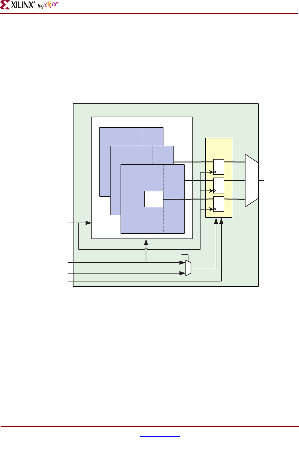
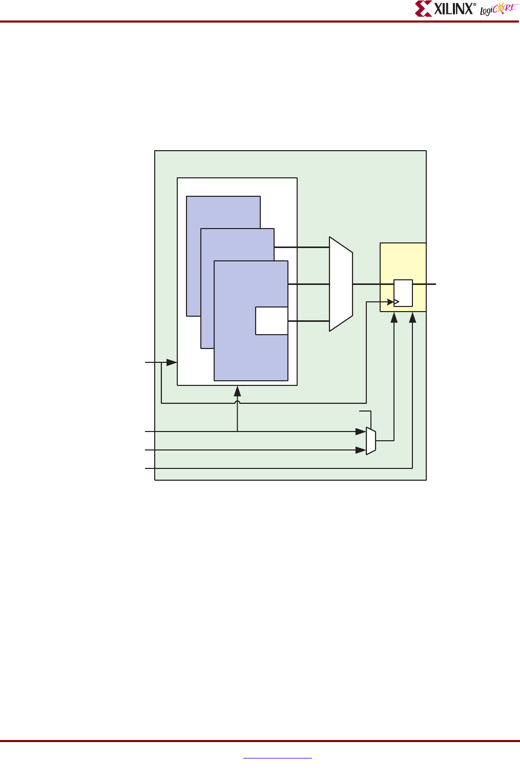
Virtex-4 Memory with Core Output Registers Only
When only the output is selected to be registered, then the core that is generated has the Virtex-4
embedded registers disabled, as shown in Figure 30.
Register output of memory primitive
; Register output of memory core
Figure Top x-ref 27
Figure 30: Virtex-4 Block Memory Generated With Core Output Registers
Block Memory Generator Core
Utilized Block RAM Primitives
Block RAM
Embedded
Output
Registers
Latches
Block RAM
Embedded
Output
Registers
Latches
Core
Output
Registers
EN
HAS_REGCE_PIN
REGCE
0
1
MUX
CLK
SSR
DOUT
Block RAM
Embedded
Output
Registers
DIsabled
Latches
Block Memory Generator v1.1
DS512 January 18, 2006 www.xilinx.com 41
Product Specification
Virtex-4 Memory with No Optional Registers
When the no optional registers are selected, then the output of memory primitive is driven directly
from the RAM primitive latches, and for cores that use more than one primitive, the output is driven
from any the multiplexers required, and shown in Figure 31.
Register output of memory primitive
Register output of memory core
Figure Top x-ref 28
Figure 31: Virtex-4 Block Memory Generated With No Optional Registers
Block Memory Generator Core
Utilized Block RAM Primitives
Block RAM
Embedded
Output
Registers
Latches
Block RAM
Embedded
Output
Registers
Latches
EN
MUX
CLK
SSR
DOUT
Block RAM
Embedded
Output
Registers
Disabled
Latches
Block Memory Generator v1.1
42 www.xilinx.com DS512 January 18, 2006
Product Specification
Non-Virtex-4: Output Register Configurations
To tailor the register options of non-Virtex-4 architectures, two check boxes are provided in the CORE
Generator GUI under the Output Pipelining section. For implementing registers on the outputs of the
individual block RAM primitives, the box labeled “Register output of memory primitive” is checked. Like-
wise, registering the output of the core is enabled by checking the box labeled “Register output of memory
core.” Illustrated below are the resulting implementations of the four permutations supported by these
configuration options.
Non-Virtex-4: Memory with Primitive and Core Output Registers
When both options are selected, then a memory core is generated with registers on the outputs of the
individual RAM primitives and on the core output, as shown in Figure 32. If you are building a large
memory construct, selecting this configuration can provide improved performance.
; Register output of memory primitive
; Register output of memory core
Figure Top x-ref 29
Figure 32: Non-Virtex-4 Memory With Both Primitive and Core Output Registers Enabled
Block Memory Generator Core
Core
Output
Registers
Latches
Latches
EN
HAS_REGCE_PIN
REGCE
Primitive
Output
Registers
0
1
MUX
Utilized Block RAM Primitives
Block RAM
Block RAM
Block RAM
Latches
CLK
SSR
DOUT
Block Memory Generator v1.1
DS512 January 18, 2006 www.xilinx.com 43
Product Specification
Non-Virtex-4: Memory with Embedded Registers Only
When the option to register the primitive is selected, then a core is generated that only registers the out-
put of the RAM primitives. Note that the output of any multiplexing required to combine multiple
primitives will be not be registered in this configuration, as shown in Figure 33.
; Register output of memory primitive
Register output of memory core
Figure Top x-ref 30
Figure 33: Non-Virtex-4 Block Memory Generated With Primitive Registers
Block Memory Generator CORE
Latches
Latches
EN
HAS_REGCE_PIN
REGCE
Primitive
Output
Registers
0
1
MUX
Utilized Block RAM Primitives
Block RAM
Block RAM
Block RAM
Latches
CLK
SSR
DOUT
Block Memory Generator v1.1
44 www.xilinx.com DS512 January 18, 2006
Product Specification
Non-Virtex-4: Memory with Core Output Registers Only
A memory that is configured with only the output registered selected is shown in Figure 34.
Register output of memory primitive
; Register output of memory core
Figure Top x-ref 31
Figure 34: Non-Virtex-4 Block Memory Generated With Core Output Registers
Block Memory Generator CORE
Core
Output
Registers
Latches
Latches
EN
HAS_REGCE_PIN
REGCE
0
1
Utilized Block RAM Primitives
Block RAM
CLK
SSR
DOUTMUX
Block RAM
Block RAM
Latches
Block Memory Generator v1.1
DS512 January 18, 2006 www.xilinx.com 45
Product Specification
Non-Virtex-4: Memory with No Optional Registers
When no output register option is selected, then the output of the memory primitive is driven directly
from the memory latches, and for cores that use more than one primitive, the core output is driven from
any multiplexers required, and shown in Figure 35.
Register output of memory primitive
Register output of memory core
Figure Top x-ref 32
Figure 35: Non-Virtex-4 Block Memory Generated With No Optional Registers
Block Memory Generator Core
Latches
Latches
EN
Utilized Block RAM Primitives
CLK
SSR
DOUTMUX
Block RAM
Block RAM
Block RAM
Latches
Block Memory Generator v1.1
46 www.xilinx.com DS512 January 18, 2006
Product Specification
Ordering Information
This free core in included with the Xilinx ISE CORE Generator system. Updates to the core are bundled
with ISE IP Updates, which are accessible from the Xilinx
Download Center. To order Xilinx software,
please contact your local Xilinx sales representative. Information on additional Xilinx LogiCORE mod-
ules is available at the Xilinx
IP Center.
Related Information
Xilinx products are not intended for use in life-support appliances, devices, or systems. Use of a Xilinx
product in such application without the written consent of the appropriate Xilinx officer is prohibited.
Revision History
Date Version Revision
01/11/06 1.0 Initial Xilinx release.
