Chapter 7: HDL Coding Techniques
RAM HDL Coding Techniques
XST extended Random Access Memory (RAM) inferencing:
• Makes it unnecessary to manually instantiate RAM primitives.
• Saves time.
• Keeps HDL source code portable and scalable.
Distributed RAM and Dedicated Block RAM
• RAM resources are of two types:
– Distributed RAM
Must be used for RAM descriptions with asynchronous read.
– Dedicated block RAM
Generally used for RAM descriptions with synchronous read.
• Use RAM Style to control RAM implementation.
• For more information, see distributed RAM and related topics in:
– V
irtex-6 FPGA Memory Resources User Guide
– Virtex-6 FPGA Congurable Logic Block User Guide
– Spartan-6 FPGA Block RAM Resources User Guide
– Spartan-6 FPGA Congurable Logic Block User Guide
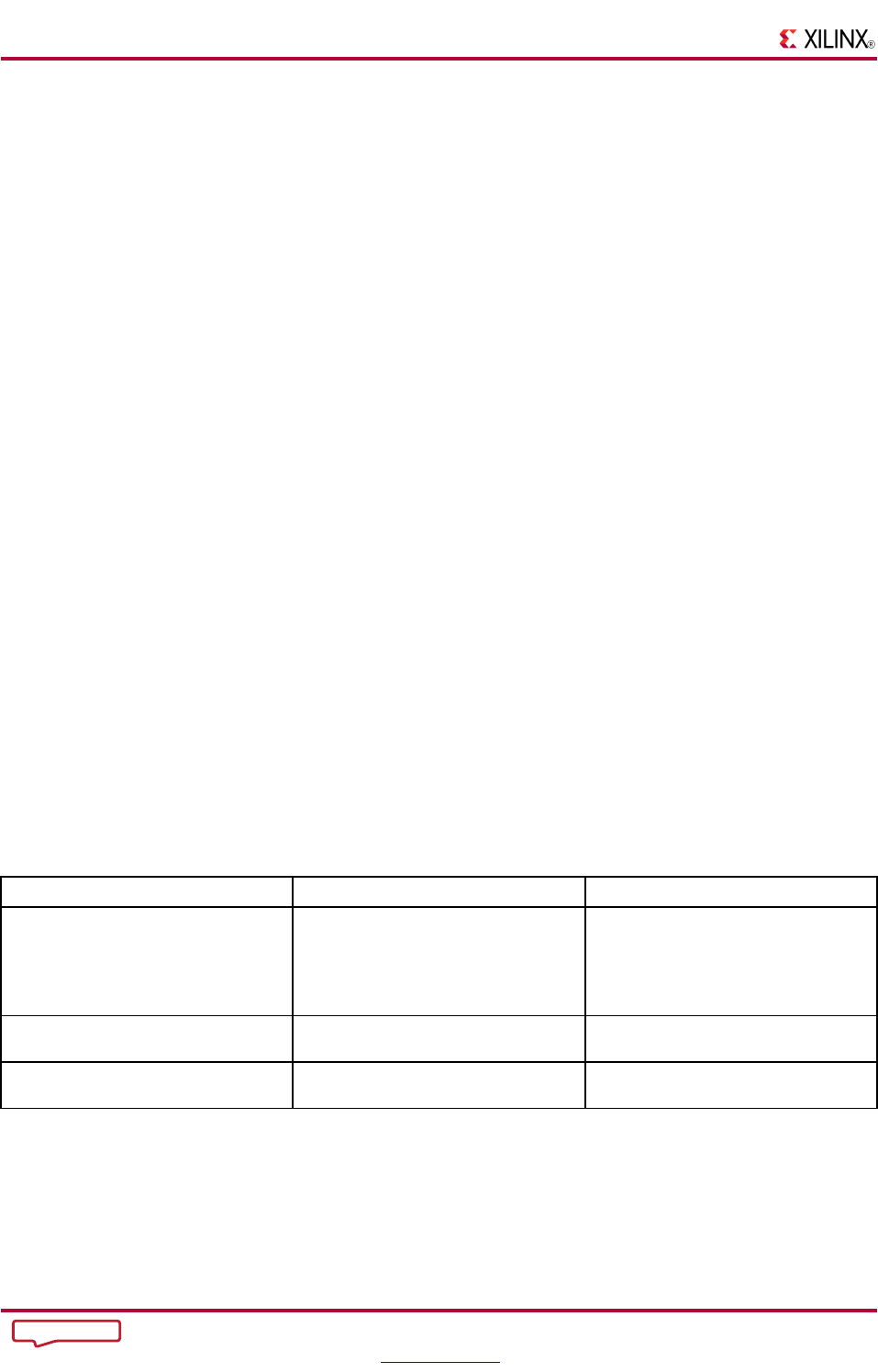
Distributed RAM and Dedicated Block RAM Comparison
Data is written synchronously into the RAM for both types. The primary difference
between distributed RAM and dedicated block RAM lies in the way data is read from the
RAM. See the following table.
Action Distributed RAM Dedicated Block Ram
Write
Synchronous Synchronous
Read Asynchronous Synchronous
Choosing Between Distributed RAM and Dedicated Block RAM
Whether to use distributed RAM or dedicated block RAM may depend on:
• The characteristics of the RAM you have described in the HDL source code
• Whether you have forced a specic implementation style
• Availability of block RAM resources
Asynchronous Read (Distributed RAM)
• RAM descriptions with asynchronous read:
– Are implemented with distributed RAM.
– Cannot be implemented in dedicated block RAM.
• Distributed RAM is implemented on properly congured slice logic.
XST User Guide for Virtex-6, Spartan-6, and 7 Series Devices
200 www.xilinx.com UG687 (v 14.5) March 20, 2013
Send Feedback

Chapter 7: HDL Coding Techniques
Synchronous Read (Dedicated Block RAM)
RAM descriptions with synchronous read:
• Generally go into dedicated block RAM.
• Are implemented using distributed RAM plus additional registers if you have so
requested, or for device resource utilization.
RAM-Supported Features
RAM-supported features include:
• RAM Inferencing Capabilities
• Parity Bits
RAM Inferencing Capabilities
RAM inferencing capabilities include the following.
• Support for any size and data width. XST maps the RAM description to one or
several RAM primitives.
• Single-port, simple-dual port, true dual port.
• Up to two write ports.
• Multiple read ports.
Provided that only one write port is described, XST can identify RAM descriptions
with two or more read ports that access the RAM contents at addresses different
from the write address.
• Simple-dual port and true dual-port RAM with asymmetric ports. For more
information, see Asymmetric Ports Support (Block RAM).
• Write enable.
• RAM enable (block RAM).
• Data output reset (block RAM).
• Optional output register (block RAM).
• Byte-Wide Write Enable (block RAM).
• Each RAM port can be controlled by its distinct clock, RAM enable, write enable,
and data output reset.
• Initial contents specication.
Parity Bits
XST does not support parity bits.
• Parity bits are available on certain block RAM primitives.
• XST can use parity bits as regular data bits in order to accommodate the described
data widths.
• XST cannot:
– Automatically generate parity control logic.
– Use those parity bit positions for their intended purpose.
XST User Guide for Virtex-6, Spartan-6, and 7 Series Devices
UG687 (v 14.5) March 20, 2013 www.xilinx.com 201
Send Feedback

Chapter 7: HDL Coding Techniques
RAM HDL Coding Guidelines
RAM HDL coding guidelines include:
• RAM Modeling
• Describing Read Access
• Block RAM Read/Write Synchronization
• Re-Settable Data Outputs (Block RAM)
• Byte-Write Enable Support (Block RAM)
• Asymmetric Ports Support
• RAM Initial Contents
RAM Modeling
RAM is usually modeled with an array of array object.
Modeling a RAM in VHDL (Single Write Port)
To model a RAM with a single write port, use a VHDL signal as follows:
type ram_type is array (0 to 255) of std_logic_vector (15 downto 0);
signal RAM : ram_type;
Modeling a RAM in VHDL (Two Write Ports)
To model a RAM with two write ports in VHDL, use a shared variable instead of a signal.
type ram_type is array (0 to 255) of std_logic_vector (15 downto 0);
shared variable RAM : ram_type;
• XST rejects an attempt to use a signal to model a RAM with two write ports. Such a
model does not behave correctly during simulation.
• Shared variables are an extension of variables, allowing inter-process
communication.
– Use shared variables with even greater caution than variables.
– Shared variables inherit all basic characteristics from variables.
– The order in which items in a sequential process are described can condition the
functionality being modeled.
– Two or more processes making assignments to a shared variable in the same
simulation cycle can lead to unpredictable results.
• Although shared variables are valid and accepted by XST, do not use a shared
variable if the RAM has only one write port. Use a signal instead.
Modeling a RAM in Verilog Coding Example
reg [15:0] RAM [0:255];
XST User Guide for Virtex-6, Spartan-6, and 7 Series Devices
202 www.xilinx.com UG687 (v 14.5) March 20, 2013
Send Feedback

Chapter 7: HDL Coding Techniques
Describing Write Access
Describing Write Access includes:
• Describing Write Access in VHDL
• Describing Write Access in Verilog
Describing Write Access in VHDL
• For a RAM modeled with a VHDL signal, write into the RAM is typically described
as follows:
process (clk)
begin
if rising_edge(clk) then
if we = ‘1’ then
RAM(conv_integer(addr)) <= di;
end if;
end if;
end process;
• The address signal is typically declared as follows:
signal addr : std_logic_vector(ADDR_WIDTH-1 downto 0);
Including std_logic_unsigned
• You must include std_logic_unsigned in order to use the conv_integer conversion
function.
• Although std_logic_signed also includes a conv_integer function, Xilinx®
recommends that you not use std_logic_signed in this instance.
• If you use std_logic_signed:
– XST assumes that address signals have a signed representation.
– XST ignores all negative values.
– An inferred RAM of half the desired size may result.
• If you need signed data representation in some parts of the design, describe them in
units separate from the RAM components.
RAM Modeled With VHDL Shared Variable Coding Example
This coding example shows a typical write description when the RAM:
• Has two write ports, and
• Is modeled with a VHDL shared variable.
process (clk)
begin
if rising_edge(clk) then
if we = ‘1’ then
RAM(conv_integer(addr)) := di;
end if;
end if;
end process;
XST User Guide for Virtex-6, Spartan-6, and 7 Series Devices
UG687 (v 14.5) March 20, 2013 www.xilinx.com 203
Send Feedback

Chapter 7: HDL Coding Techniques
Describing Write Access in Verilog
always @ (posedge clk)
begin
if (we)
RAM[addr] <= di;
end
Describing Read Access
Describing Read Access includes:
• Describing Read Access in VHDL
• Describing Read Access in Verilog
Describing Read Access in VHDL
• A RAM component is typically read-accessed at a given address location.
do <= RAM( conv_integer(addr));
• Whether this statement is a simple concurrent statement, or is described in a
sequential process, determines whether :
– The read is asynchronous or synchronous.
– The RAM component is implemented using:
♦ block RAM resources, or
♦ distributed RAM resources
• For more information, see Block RAM Read/Write Synchronization.
RAM Implemented on Block Resources Coding Example
process (clk)
begin
do <= RAM( conv_integer(addr));
end process;
Describing Read Access in Verilog
• Describe an asynchronous read with an assign statement.
assign do = RAM[addr];
• Describe a synchronous read with a sequential always block.
always @ (posedge clk)
begin
do <= RAM[addr];
end
• For more information, see Block RAM Read/Write Synchronization.
XST User Guide for Virtex-6, Spartan-6, and 7 Series Devices
204 www.xilinx.com UG687 (v 14.5) March 20, 2013
Send Feedback

Chapter 7: HDL Coding Techniques
Block RAM Read/Write Synchronization
• You can congure Block RAM resources to provide the following synchronization
modes for a given read/write port:
– Read-rst
Old content is read before new content is loaded.
– Write-rst
♦ New content is immediately made available for reading.
♦ Write-rst is also known as read-through.
– No-change
Data output does not change as new content is loaded into RAM.
• XST provides inference support for all of these synchronization modes. You can
describe a different synchronization mode for each port of the RAM.
• When one port performs a write operation, the write operation succeeds. The other
port can reliably read data from the same location if the write port is in Read-rst
mode. DATA_OUT on both ports will then reect the previously stored data.
• In Read-rst mode for BRAM SDP conguration, if read and write access the same
memory location at the same time during synchronous clocking, there will be a
simulation mismatch.
Block RAM Read/Write Synchronization VHDL Coding Example One
process (clk)
begin
if (clk’event and clk = ’1’) then
if (we = ’1’) then
RAM(conv_integer(addr)) <= di;
end if;
do <= RAM(conv_integer(addr));
end if;
end process;
Block RAM Read/Write Synchronization VHDL Coding Example Two
This coding example describes a write-rst synchronized port.
process (clk)
begin
if (clk’event and clk = ’1’) then
if (we = ’1’) then
RAM(conv_integer(addr)) <= di;
do <= di;
else
do <= RAM(conv_integer(addr));
end if;
end if;
end process;
XST User Guide for Virtex-6, Spartan-6, and 7 Series Devices
UG687 (v 14.5) March 20, 2013 www.xilinx.com 205
Send Feedback

Chapter 7: HDL Coding Techniques
Block RAM Read/Write Synchronization VHDL Coding Example Three
This coding example describes a no-change synchronization.
process (clk)
begin
if (clk’event and clk = ’1’) then
if (we = ’1’) then
RAM(conv_integer(addr)) <= di;
else
do <= RAM(conv_integer(addr));
end if;
end if;
end process;
Block RAM Read/Write Synchronization VHDL Coding Example Four
Caution! If you model a dual-write RAM with a VHDL shared variable, be aware that
the synchronization described below is not read-rst, but write-rst.
process (clk)
begin
if (clk’event and clk = ’1’) then
if (we = ’1’) then
RAM(conv_integer(addr)) := di;
end if;
do <= RAM(conv_integer(addr));
end if;
end process;
Block RAM Read/Write Synchronization VHDL Coding Example Five
To describe a read-rst synchronization, reorder the process body.
process (clk)
begin
if (clk’event and clk = ’1’) then
do <= RAM(conv_integer(addr));
if (we = ’1’) then
RAM(conv_integer(addr)) := di;
end if;
end if;
end process;
Re-Settable Data Outputs (Block RAM)
You can optionally describe a reset to any constant value of synchronously read data.
• XST recognizes the reset and takes advantage of the synchronous set/reset feature of
block RAM components.
• For a RAM port with read-rst synchronization, describe the reset functionality as
shown in the following coding example.
XST User Guide for Virtex-6, Spartan-6, and 7 Series Devices
206 www.xilinx.com UG687 (v 14.5) March 20, 2013
Send Feedback

Chapter 7: HDL Coding Techniques
Re-Settable Data Outputs (Block RAM) Coding Example
process (clk)
begin
if clk’event and clk = ’1’ then
if en = ’1’ then -- optional RAM enable
if we = ’1’ then -- write enable
ram(conv_integer(addr)) <= di;
end if;
if rst = ’1’ then -- optional dataout reset
do <= "00011101";
else
do <= ram(conv_integer(addr));
end if;
end if;
end if;
end process;
Byte-Wide Write Enable (Block RAM)
Xilinx® supports byte-wide write enable in block RAM.
• Use byte-wide write enable in block RAM to:
– Exercise advanced control over writing data into RAM.
– Separately specify the writeable portions of 8 bits of an addressed memory.
• From the standpoint of HDL modeling and inference, the concept is best described
as a column-based write.
– The RAM is seen as a collection of equal size columns.
– During a write cycle, you separately control writing into each of these columns.
• XST inferencing allows you to take advantage of the block RAM byte-wide enable
feature.
• XST supports two description styles:
– Single-Process Description Style (Recommended)
– Two-Process Description Style (Not Recommended)
Single-Process Description Style (Recommended)
The Single-Process Description Style is more intuitive and less error-prone than the
Two-Process Description Style.
The described RAM is implemented on block RAM resources, using the byte-write
enable capability, provided that the following requirements are met.
• Write columns of equal widths
• Allowed write column widths: 8-bit, 9-bit, 16-bit, 18-bit
For other write column widths, such as 5-bit or 12-bit, XST uses distributed RAM
resources and creates additional multiplexing logic on the data input.
• Number of write columns: any
• RAM depth: any
XST implements the RAM using one or several block RAM primitives as needed.
• Supported read-write synchronizations: read-rst, write-rst, no-change
XST User Guide for Virtex-6, Spartan-6, and 7 Series Devices
UG687 (v 14.5) March 20, 2013 www.xilinx.com 207
Send Feedback

Chapter 7: HDL Coding Techniques
Single-Process Description Style VHDL Coding Example
This coding example uses generics and a for-loop construct for a compact and easily
changeable conguration of the desired number and width of write columns.
--
-- Single-Port BRAM with Byte-wide Write Enable
-- 2x8-bit write
-- Read-First mode
-- Single-process description
-- Compact description of the write with a for-loop statement
-- Column width and number of columns easily configurable
--
--
-- Download: http://www.xilinx.com/txpatches/pub/documentation/misc/xstug_examples.zip
-- File: HDL_Coding_Techniques/rams/bytewrite_ram_1b.vhd
--
library ieee;
use ieee.std_logic_1164.all;
use ieee.std_logic_unsigned.all;
entity bytewrite_ram_1b is
generic (
SIZE : integer := 1024;
ADDR_WIDTH : integer := 10;
COL_WIDTH : integer := 8;
NB_COL : integer := 2);
port (
clk : in std_logic;
we : in std_logic_vector(NB_COL-1 downto 0);
addr : in std_logic_vector(ADDR_WIDTH-1 downto 0);
di : in std_logic_vector(NB_COL*COL_WIDTH-1 downto 0);
do : out std_logic_vector(NB_COL*COL_WIDTH-1 downto 0));
end bytewrite_ram_1b;
architecture behavioral of bytewrite_ram_1b is
type ram_type is array (SIZE-1 downto 0)
of std_logic_vector (NB_COL*COL_WIDTH-1 downto 0);
signal RAM : ram_type := (others => (others => ’0’));
begin
process (clk)
begin
if rising_edge(clk) then
do <= RAM(conv_integer(addr));
for i in 0 to NB_COL-1 loop
if we(i) = ’1’ then
RAM(conv_integer(addr))((i+1)*COL_WIDTH-1 downto i*COL_WIDTH)
<= di((i+1)*COL_WIDTH-1 downto i*COL_WIDTH);
end if;
end loop;
end if;
end process;
end behavioral;
XST User Guide for Virtex-6, Spartan-6, and 7 Series Devices
208 www.xilinx.com UG687 (v 14.5) March 20, 2013
Send Feedback

Chapter 7: HDL Coding Techniques
Single-Process Description Style Verilog Coding Example
This coding example uses parameters and a generate-for construct.
//
// Single-Port BRAM with Byte-wide Write Enable
// 4x9-bit write
// Read-First mode
// Single-process description
// Compact description of the write with a generate-for statement
// Column width and number of columns easily configurable
//
// Download: http://www.xilinx.com/txpatches/pub/documentation/misc/xstug_examples.zip
// File: HDL_Coding_Techniques/rams/bytewrite_ram_1b.v
//
module v_bytewrite_ram_1b (clk, we, addr, di, do);
parameter SIZE = 1024;
parameter ADDR_WIDTH = 10;
parameter COL_WIDTH = 9;
parameter NB_COL = 4;
input clk;
input [NB_COL-1:0] we;
input [ADDR_WIDTH-1:0] addr;
input [NB_COL*COL_WIDTH-1:0] di;
output reg [NB_COL*COL_WIDTH-1:0] do;
reg [NB_COL*COL_WIDTH-1:0] RAM [SIZE-1:0];
always @(posedge clk)
begin
do <= RAM[addr];
end
generate
genvar i;
for (i = 0; i < NB_COL; i = i+1)
begin
always @(posedge clk)
begin
if (we[i])
RAM[addr][(i+1)*COL_WIDTH-1:i*COL_WIDTH] <= di[(i+1)*COL_WIDTH-1:i*COL_WIDTH];
end
end
endgenerate
endmodule
XST User Guide for Virtex-6, Spartan-6, and 7 Series Devices
UG687 (v 14.5) March 20, 2013 www.xilinx.com 209
Send Feedback

Chapter 7: HDL Coding Techniques
Single-Process Description Style for No-Change VHDL Coding Example
The Single-Process Description Style is the only way to correctly model byte-write
enable functionality in conjunction with no-change read-write synchronization.
--
-- Single-Port BRAM with Byte-wide Write Enable
-- 2x8-bit write
-- No-Change mode
-- Single-process description
-- Compact description of the write with a for-loop statement
-- Column width and number of columns easily configurable
--
--
-- Download: http://www.xilinx.com/txpatches/pub/documentation/misc/xstug_examples.zip
-- File: HDL_Coding_Techniques/rams/bytewrite_nochange.vhd
--
library ieee;
use ieee.std_logic_1164.all;
use ieee.std_logic_unsigned.all;
entity bytewrite_nochange is
generic (
SIZE : integer := 1024;
ADDR_WIDTH : integer := 10;
COL_WIDTH : integer := 8;
NB_COL : integer := 2);
port (
clk : in std_logic;
we : in std_logic_vector(NB_COL-1 downto 0);
addr : in std_logic_vector(ADDR_WIDTH-1 downto 0);
di : in std_logic_vector(NB_COL*COL_WIDTH-1 downto 0);
do : out std_logic_vector(NB_COL*COL_WIDTH-1 downto 0));
end bytewrite_nochange;
architecture behavioral of bytewrite_nochange is
type ram_type is array (SIZE-1 downto 0) of std_logic_vector (NB_COL*COL_WIDTH-1 downto 0);
signal RAM : ram_type := (others => (others => ’0’));
begin
process (clk)
begin
if rising_edge(clk) then
if (we = (we’range => ’0’)) then
do <= RAM(conv_integer(addr));
end if;
for i in 0 to NB_COL-1 loop
if we(i) = ’1’ then
RAM(conv_integer(addr))((i+1)*COL_WIDTH-1 downto i*COL_WIDTH)
<= di((i+1)*COL_WIDTH-1 downto i*COL_WIDTH);
end if;
end loop;
end if;
end process;
end behavioral;
XST User Guide for Virtex-6, Spartan-6, and 7 Series Devices
210 www.xilinx.com UG687 (v 14.5) March 20, 2013
Send Feedback

Chapter 7: HDL Coding Techniques
Single-Process Description Style for No-Change Verilog Coding Example
//
// Single-Port BRAM with Byte-wide Write Enable
// 4x9-bit write
// No-Change mode
// Single-process description
// Compact description of the write with a generate-for statement
// Column width and number of columns easily configurable
//
// Download: http://www.xilinx.com/txpatches/pub/documentation/misc/xstug_examples.zip
// File: HDL_Coding_Techniques/rams/bytewrite_nochange.v
//
module v_bytewrite_nochange (clk, we, addr, di, do);
parameter SIZE = 1024;
parameter ADDR_WIDTH = 10;
parameter COL_WIDTH = 9;
parameter NB_COL = 4;
input clk;
input [NB_COL-1:0] we;
input [ADDR_WIDTH-1:0] addr;
input [NB_COL*COL_WIDTH-1:0] di;
output reg [NB_COL*COL_WIDTH-1:0] do;
reg [NB_COL*COL_WIDTH-1:0] RAM [SIZE-1:0];
always @(posedge clk)
begin
if (~|we)
do <= RAM[addr];
end
generate
genvar i;
for (i = 0; i < NB_COL; i = i+1)
begin
always @(posedge clk)
begin
if (we[i])
RAM[addr][(i+1)*COL_WIDTH-1:i*COL_WIDTH]
<= di[(i+1)*COL_WIDTH-1:i*COL_WIDTH];
end
end
endgenerate
endmodule
XST User Guide for Virtex-6, Spartan-6, and 7 Series Devices
UG687 (v 14.5) March 20, 2013 www.xilinx.com 211
Send Feedback

Chapter 7: HDL Coding Techniques
Two-Process Description Style
In order to take advantage of block RAM byte-write enable capabilities, you must
provide adequate data read synchronization. If you do not do so, XST implements the
described functionality sub-optimally, using distributed RAM resources instead.
• The Two-Process Description Style continues to be supported, but is no longer
recommended.
• The Two-Process Description Style does not allow you to properly describe
byte-write enable functionality in conjunction with the no-change synchronization
mode.
• Xilinx recommends:
– If you currently use the Two-Process Description Style, change your design to
the Single-Process Description Style.
– Do not use the Two-Process Description Style for new designs.
• If you are unable to migrate your code to the Single-Process Description Style, XST
still supports the Two-Process Description Style.
• In the Two-Process Description Style:
– A combinatorial process describes which data is loaded and read for each byte.
In particular, the write enable functionality is described there, and not in the
main sequential process.
– A sequential process describes the write and read synchronization.
– Data widths are more restrictive than with the Single-Process Description Style:
♦ Number of write columns: 2 or 4
♦ Write column widths: 8-bit or 9-bit
♦ Supported data widths: 2x8-bit (two columns of 8 bits each), 2x9-bit, 4x8-bit,
4x9-bit
XST User Guide for Virtex-6, Spartan-6, and 7 Series Devices
212 www.xilinx.com UG687 (v 14.5) March 20, 2013
Send Feedback

Chapter 7: HDL Coding Techniques
Two-Process Description Style VHDL Coding Example
--
-- Single-Port BRAM with Byte-wide Write Enable
-- 2x8-bit write
-- Read-First Mode
-- Two-process description
--
-- Download: http://www.xilinx.com/txpatches/pub/documentation/misc/xstug_examples.zip
-- File: HDL_Coding_Techniques/rams/rams_24.vhd
--
library ieee;
use ieee.std_logic_1164.all;
use ieee.std_logic_unsigned.all;
entity rams_24 is
generic (
SIZE : integer := 512;
ADDR_WIDTH : integer := 9;
COL_WIDTH : integer := 16;
NB_COL : integer := 2);
port (
clk : in std_logic;
we : in std_logic_vector(NB_COL-1 downto 0);
addr : in std_logic_vector(ADDR_WIDTH-1 downto 0);
di : in std_logic_vector(NB_COL*COL_WIDTH-1 downto 0);
do : out std_logic_vector(NB_COL*COL_WIDTH-1 downto 0));
end rams_24;
architecture syn of rams_24 is
type ram_type is array (SIZE-1 downto 0) of std_logic_vector (NB_COL*COL_WIDTH-1 downto 0);
signal RAM : ram_type := (others => (others => ’0’));
signal di0, di1 : std_logic_vector (COL_WIDTH-1 downto 0);
begin
process(we, di)
begin
if we(1) = ’1’ then
di1 <= di(2*COL_WIDTH-1 downto 1*COL_WIDTH);
else
di1 <= RAM(conv_integer(addr))(2*COL_WIDTH-1 downto 1*COL_WIDTH);
end if;
if we(0) = ’1’ then
di0 <= di(COL_WIDTH-1 downto 0);
else
di0 <= RAM(conv_integer(addr))(COL_WIDTH-1 downto 0);
end if;
end process;
process(clk)
begin
if (clk’event and clk = ’1’) then
do <= RAM(conv_integer(addr));
RAM(conv_integer(addr)) <= di1 & di0;
end if;
end process;
end syn;
XST User Guide for Virtex-6, Spartan-6, and 7 Series Devices
UG687 (v 14.5) March 20, 2013 www.xilinx.com 213
Send Feedback

Chapter 7: HDL Coding Techniques
Two-Process Description Style Verilog Coding Example
//
// Single-Port BRAM with Byte-wide Write Enable (2 bytes) in Read-First Mode
//
// Download: http://www.xilinx.com/txpatches/pub/documentation/misc/xstug_examples.zip
// File: HDL_Coding_Techniques/rams/rams_24.v
//
module v_rams_24 (clk, we, addr, di, do);
parameter SIZE = 512;
parameter ADDR_WIDTH = 9;
parameter DI_WIDTH = 8;
input clk;
input [1:0] we;
input [ADDR_WIDTH-1:0] addr;
input [2*DI_WIDTH-1:0] di;
output [2*DI_WIDTH-1:0] do;
reg [2*DI_WIDTH-1:0] RAM [SIZE-1:0];
reg [2*DI_WIDTH-1:0] do;
reg [DI_WIDTH-1:0] di0, di1;
always @(we or di)
begin
if (we[1])
di1 = di[2*DI_WIDTH-1:1*DI_WIDTH];
else
di1 = RAM[addr][2*DI_WIDTH-1:1*DI_WIDTH];
if (we[0])
di0 = di[DI_WIDTH-1:0];
else
di0 = RAM[addr][DI_WIDTH-1:0];
end
always @(posedge clk)
begin
do <= RAM[addr];
RAM[addr]<={di1,di0};
end
endmodule
XST User Guide for Virtex-6, Spartan-6, and 7 Series Devices
214 www.xilinx.com UG687 (v 14.5) March 20, 2013
Send Feedback

Chapter 7: HDL Coding Techniques
Asymmetric Ports Support (Block RAM)
Block RAM resources can be congured with two asymmetric ports.
• Port A accesses the physical memory with a specic data width.
• Port B accesses the same physical memory with a different data width.
• Both ports access the same physical memory, but see a different logical organization
of the RAM. For example, the same 2048 bits of physical memory may be seen as:
– 256x8-bit by Port A
– 64x32-bit by Port B
• Such an asymmetrically congured block RAM is said to have ports with different
aspect ratios.
• A typical use of port asymmetry is to create storage and buffering between two data
ows. The data ows:
– Have different data width characteristics.
– Operate at asymmetric speeds.
Note Asymmetric RAM inference for data buses larger than 18-bit will require the
RAMB36E1 block.
Block RAM With Asymmetric Ports Modeling
Like RAM with no port asymmetry, block RAM with asymmetric ports is modeled
with a single array of array object.
• The depth and width characteristics of the modeling signal or shared variable match
the RAM port with the lower data width (subsequently the larger depth).
• As a result of this modeling requirement, describing a read or write access for the
port with the larger data width no longer implies one assignment, but several
assignments.
– The number of assignments equals the ratio between the two asymmetric data
widths.
– Each of these assignments may be explicitly described as illustrated in the
following coding examples.
XST User Guide for Virtex-6, Spartan-6, and 7 Series Devices
UG687 (v 14.5) March 20, 2013 www.xilinx.com 215
Send Feedback

Chapter 7: HDL Coding Techniques
Asymmetric Port RAM VHDL Coding Example
--
-- Asymmetric port RAM
-- Port A is 256x8-bit write-only
-- Port B is 64x32-bit read-only
--
-- Download: http://www.xilinx.com/txpatches/pub/documentation/misc/xstug_examples.zip
-- File: HDL_Coding_Techniques/rams/asymmetric_ram_1a.vhd
--
library ieee;
use ieee.std_logic_1164.all;
use ieee.std_logic_unsigned.all;
use ieee.std_logic_arith.all;
entity asymmetric_ram_1a is
generic (
WIDTHA : integer := 8;
SIZEA : integer := 256;
ADDRWIDTHA : integer := 8;
WIDTHB : integer := 32;
SIZEB : integer := 64;
ADDRWIDTHB : integer := 6
);
port (
clkA : in std_logic;
clkB : in std_logic;
weA : in std_logic;
enA : in std_logic;
enB : in std_logic;
addrA : in std_logic_vector(ADDRWIDTHA-1 downto 0);
addrB : in std_logic_vector(ADDRWIDTHB-1 downto 0);
diA : in std_logic_vector(WIDTHA-1 downto 0);
doB : out std_logic_vector(WIDTHB-1 downto 0)
);
end asymmetric_ram_1a;
architecture behavioral of asymmetric_ram_1a is
function max(L, R: INTEGER) return INTEGER is
begin
if L > R then
return L;
else
return R;
end if;
end;
function min(L, R: INTEGER) return INTEGER is
begin
if L < R then
return L;
else
return R;
end if;
end;
constant minWIDTH : integer := min(WIDTHA,WIDTHB);
constant maxWIDTH : integer := max(WIDTHA,WIDTHB);
constant maxSIZE : integer := max(SIZEA,SIZEB);
constant RATIO : integer := maxWIDTH / minWIDTH;
type ramType is array (0 to maxSIZE-1) of std_logic_vector(minWIDTH-1 downto 0);
signal ram : ramType := (others => (others => ’0’));
signal readB : std_logic_vector(WIDTHB-1 downto 0):= (others => ’0’);
signal regB : std_logic_vector(WIDTHB-1 downto 0):= (others => ’0’);
begin
XST User Guide for Virtex-6, Spartan-6, and 7 Series Devices
216 www.xilinx.com UG687 (v 14.5) March 20, 2013
Send Feedback

Chapter 7: HDL Coding Techniques
process (clkA)
begin
if rising_edge(clkA) then
if enA = ’1’ then
if weA = ’1’ then
ram(conv_integer(addrA)) <= diA;
end if;
end if;
end if;
end process;
process (clkB)
begin
if rising_edge(clkB) then
if enB = ’1’ then
readB(minWIDTH-1 downto 0)
<= ram(conv_integer(addrB&conv_std_logic_vector(0,2)));
readB(2*minWIDTH-1 downto minWIDTH)
<= ram(conv_integer(addrB&conv_std_logic_vector(1,2)));
readB(3*minWIDTH-1 downto 2*minWIDTH)
<= ram(conv_integer(addrB&conv_std_logic_vector(2,2)));
readB(4*minWIDTH-1 downto 3*minWIDTH)
<= ram(conv_integer(addrB&conv_std_logic_vector(3,2)));
end if;
regB <= readB;
end if;
end process;
doB <= regB;
end behavioral;
XST User Guide for Virtex-6, Spartan-6, and 7 Series Devices
UG687 (v 14.5) March 20, 2013 www.xilinx.com 217
Send Feedback

Chapter 7: HDL Coding Techniques
Asymmetric Port RAM Verilog Coding Example
//
// Asymmetric port RAM
// Port A is 256x8-bit write-only
// Port B is 64x32-bit read-only
//
// Download: http://www.xilinx.com/txpatches/pub/documentation/misc/xstug_examples.zip
// File: HDL_Coding_Techniques/rams/asymmetric_ram_1a.v
//
module v_asymmetric_ram_1a (clkA, clkB, weA, reB, addrA, addrB, diA, doB);
parameter WIDTHA = 8;
parameter SIZEA = 256;
parameter ADDRWIDTHA = 8;
parameter WIDTHB = 32;
parameter SIZEB = 64;
parameter ADDRWIDTHB = 6;
input clkA;
input clkB;
input weA;
input reB;
input [ADDRWIDTHA-1:0] addrA;
input [ADDRWIDTHB-1:0] addrB;
input [WIDTHA-1:0] diA;
output reg [WIDTHB-1:0] doB;
‘define max(a,b) {(a) > (b) ? (a) : (b)}
‘define min(a,b) {(a) < (b) ? (a) : (b)}
localparam maxSIZE = ‘max(SIZEA, SIZEB);
localparam maxWIDTH = ‘max(WIDTHA, WIDTHB);
localparam minWIDTH = ‘min(WIDTHA, WIDTHB);
localparam RATIO = maxWIDTH / minWIDTH;
reg [minWIDTH-1:0] RAM [0:maxSIZE-1];
reg [WIDTHB-1:0] readB;
always @(posedge clkA)
begin
if (weA)
RAM[addrA] <= diA;
end
always @(posedge clkB)
begin
if (reB)
begin
doB <= readB;
readB[4*minWIDTH-1:3*minWIDTH] <= RAM[{addrB, 2’d3}];
readB[3*minWIDTH-1:2*minWIDTH] <= RAM[{addrB, 2’d2}];
readB[2*minWIDTH-1:minWIDTH] <= RAM[{addrB, 2’d1}];
readB[minWIDTH-1:0] <= RAM[{addrB, 2’d0}];
end
end
endmodule
XST User Guide for Virtex-6, Spartan-6, and 7 Series Devices
218 www.xilinx.com UG687 (v 14.5) March 20, 2013
Send Feedback
Chapter 7: HDL Coding Techniques
Using For-Loop Statements
Use a for-loop statement to make your VHDL code:
• More compact
• Easier to maintain
• Easier to scale
VHDL Coding Example Using For-Loop Statement
--
-- Asymmetric port RAM
-- Port A is 256x8-bit write-only
-- Port B is 64x32-bit read-only
-- Compact description with a for-loop statement
--
-- Download: http://www.xilinx.com/txpatches/pub/documentation/misc/xstug_examples.zip
-- File: HDL_Coding_Techniques/rams/asymmetric_ram_1b.vhd
--
library ieee;
use ieee.std_logic_1164.all;
use ieee.std_logic_unsigned.all;
use ieee.std_logic_arith.all;
entity asymmetric_ram_1b is
generic (
WIDTHA : integer := 8;
SIZEA : integer := 256;
ADDRWIDTHA : integer := 8;
WIDTHB : integer := 32;
SIZEB : integer := 64;
ADDRWIDTHB : integer := 6
);
port (
clkA : in std_logic;
clkB : in std_logic;
weA : in std_logic;
enA : in std_logic;
enB : in std_logic;
addrA : in std_logic_vector(ADDRWIDTHA-1 downto 0);
addrB : in std_logic_vector(ADDRWIDTHB-1 downto 0);
diA : in std_logic_vector(WIDTHA-1 downto 0);
doB : out std_logic_vector(WIDTHB-1 downto 0)
);
end asymmetric_ram_1b;
architecture behavioral of asymmetric_ram_1b is
function max(L, R: INTEGER) return INTEGER is
begin
if L > R then
return L;
else
return R;
end if;
end;
function min(L, R: INTEGER) return INTEGER is
begin
if L < R then
return L;
else
return R;
end if;
end;
function log2 (val: natural) return natural is
variable res : natural;
XST User Guide for Virtex-6, Spartan-6, and 7 Series Devices
UG687 (v 14.5) March 20, 2013 www.xilinx.com 219
Send Feedback

Chapter 7: HDL Coding Techniques
begin
for i in 30 downto 0 loop
if (val >= (2**i)) then
res := i;
exit;
end if;
end loop;
return res;
end function log2;
constant minWIDTH : integer := min(WIDTHA,WIDTHB);
constant maxWIDTH : integer := max(WIDTHA,WIDTHB);
constant maxSIZE : integer := max(SIZEA,SIZEB);
constant RATIO : integer := maxWIDTH / minWIDTH;
type ramType is array (0 to maxSIZE-1) of std_logic_vector(minWIDTH-1 downto 0);
signal ram : ramType := (others => (others => ’0’));
signal readB : std_logic_vector(WIDTHB-1 downto 0):= (others => ’0’);
signal regB : std_logic_vector(WIDTHB-1 downto 0):= (others => ’0’);
begin
process (clkA)
begin
if rising_edge(clkA) then
if enA = ’1’ then
if weA = ’1’ then
ram(conv_integer(addrA)) <= diA;
end if;
end if;
end if;
end process;
process (clkB)
begin
if rising_edge(clkB) then
if enB = ’1’ then
for i in 0 to RATIO-1 loop
readB((i+1)*minWIDTH-1 downto i*minWIDTH)
<= ram(conv_integer(addrB & conv_std_logic_vector(i,log2(RATIO))));
end loop;
end if;
regB <= readB;
end if;
end process;
doB <= regB;
end behavioral;
Verilog Coding Example Using Parameters and Generate-For Statement
Use parameters and a generate-for statement to make your Verilog code:
• More compact
• Easier to modify
//
// Asymmetric port RAM
// Port A is 256x8-bit write-only
// Port B is 64x32-bit read-only
//
// Download: http://www.xilinx.com/txpatches/pub/documentation/misc/xstug_examples.zip
// File: HDL_Coding_Techniques/rams/v_asymmetric_ram_1b.v
//
module v_asymmetric_ram_1b (clkA, clkB, weA, reB, addrA, addrB, diA, doB);
parameter WIDTHA = 8;
parameter SIZEA = 256;
parameter ADDRWIDTHA = 8;
XST User Guide for Virtex-6, Spartan-6, and 7 Series Devices
220 www.xilinx.com UG687 (v 14.5) March 20, 2013
Send Feedback

Chapter 7: HDL Coding Techniques
parameter WIDTHB = 32;
parameter SIZEB = 64;
parameter ADDRWIDTHB = 6;
input clkA;
input clkB;
input weA;
input reB;
input [ADDRWIDTHA-1:0] addrA;
input [ADDRWIDTHB-1:0] addrB;
input [WIDTHA-1:0] diA;
output reg [WIDTHB-1:0] doB;
‘define max(a,b) {(a) > (b) ? (a) : (b)}
‘define min(a,b) {(a) < (b) ? (a) : (b)}
function integer log2;
input integer value;
reg [31:0] shifted;
integer res;
begin
if (value < 2)
log2 = value;
else
begin
shifted = value-1;
for (res=0; shifted>0; res=res+1)
shifted = shifted>>1;
log2 = res;
end
end
endfunction
localparam maxSIZE = ‘max(SIZEA, SIZEB);
localparam maxWIDTH = ‘max(WIDTHA, WIDTHB);
localparam minWIDTH = ‘min(WIDTHA, WIDTHB);
localparam RATIO = maxWIDTH / minWIDTH;
localparam log2RATIO = log2(RATIO);
reg [minWIDTH-1:0] RAM [0:maxSIZE-1];
reg [WIDTHB-1:0] readB;
genvar i;
always @(posedge clkA)
begin
if (weA)
RAM[addrA] <= diA;
end
always @(posedge clkB)
begin
if (reB)
doB <= readB;
end
generate for (i = 0; i < RATIO; i = i+1)
begin: ramread
localparam [log2RATIO-1:0] lsbaddr = i;
always @(posedge clkB)
begin
readB[(i+1)*minWIDTH-1:i*minWIDTH] <= RAM[{addrB, lsbaddr}];
end
end
endgenerate
endmodule
Note These coding examples use min, max, and log2 functions to make the code as
generic and clean as possible. Those functions can be dened anywhere in the design,
typically in a package.
XST User Guide for Virtex-6, Spartan-6, and 7 Series Devices
UG687 (v 14.5) March 20, 2013 www.xilinx.com 221
Send Feedback

Chapter 7: HDL Coding Techniques
Shared Variable (VHDL)
• When you describe a symmetric port RAM in VHDL, a shared variable is required
only if you describe two ports writing into the RAM. Otherwise, a signal is preferred.
• When you describe an asymmetric port RAM in VHDL, a shared variable may be
required even if only one write port is described. If the write port has the larger data
width, several write assignments are needed to describe it, and a shared variable is
therefore required as shown in the following coding example.
Shared Variable Required VHDL Coding Example
--
-- Asymmetric port RAM
-- Port A is 256x8-bit read-only
-- Port B is 64x32-bit write-only
-- Compact description with a for-loop statement
-- A shared variable is necessary because of the multiple write assignments
--
-- Download: http://www.xilinx.com/txpatches/pub/documentation/misc/xstug_examples.zip
-- File: HDL_Coding_Techniques/rams/asymmetric_ram_4.vhd
--
library ieee;
use ieee.std_logic_1164.all;
use ieee.std_logic_unsigned.all;
use ieee.std_logic_arith.all;
entity asymmetric_ram_4 is
generic (
WIDTHA : integer := 8;
SIZEA : integer := 256;
ADDRWIDTHA : integer := 8;
WIDTHB : integer := 32;
SIZEB : integer := 64;
ADDRWIDTHB : integer := 6
);
port (
clkA : in std_logic;
clkB : in std_logic;
reA : in std_logic;
weB : in std_logic;
addrA : in std_logic_vector(ADDRWIDTHA-1 downto 0);
addrB : in std_logic_vector(ADDRWIDTHB-1 downto 0);
diB : in std_logic_vector(WIDTHB-1 downto 0);
doA : out std_logic_vector(WIDTHA-1 downto 0)
);
end asymmetric_ram_4;
architecture behavioral of asymmetric_ram_4 is
function max(L, R: INTEGER) return INTEGER is
begin
if L > R then
return L;
else
return R;
end if;
end;
function min(L, R: INTEGER) return INTEGER is
begin
if L < R then
return L;
else
return R;
end if;
end;
XST User Guide for Virtex-6, Spartan-6, and 7 Series Devices
222 www.xilinx.com UG687 (v 14.5) March 20, 2013
Send Feedback

Chapter 7: HDL Coding Techniques
function log2 (val: natural) return natural is
variable res : natural;
begin
for i in 30 downto 0 loop
if (val >= (2**i)) then
res := i;
exit;
end if;
end loop;
return res;
end function log2;
constant minWIDTH : integer := min(WIDTHA,WIDTHB);
constant maxWIDTH : integer := max(WIDTHA,WIDTHB);
constant maxSIZE : integer := max(SIZEA,SIZEB);
constant RATIO : integer := maxWIDTH / minWIDTH;
type ramType is array (0 to maxSIZE-1) of std_logic_vector(minWIDTH-1 downto 0);
shared variable ram : ramType := (others => (others => ’0’));
signal readA : std_logic_vector(WIDTHA-1 downto 0):= (others => ’0’);
signal regA : std_logic_vector(WIDTHA-1 downto 0):= (others => ’0’);
begin
process (clkA)
begin
if rising_edge(clkA) then
if reA = ’1’ then
readA <= ram(conv_integer(addrA));
end if;
regA <= readA;
end if;
end process;
process (clkB)
begin
if rising_edge(clkB) then
if weB = ’1’ then
for i in 0 to RATIO-1 loop
ram(conv_integer(addrB & conv_std_logic_vector(i,log2(RATIO))))
:= diB((i+1)*minWIDTH-1 downto i*minWIDTH);
end loop;
end if;
end if;
end process;
doA <= regA;
end behavioral;
Caution! Shared variables are an extension of variables, from which they inherit all
basic characteristics, allowing inter-process communication. Use them with great
caution.
• The order in which items in a sequential process are described can condition the
functionality being modeled.
• Two or more processes making assignments to a shared variable in the same
simulation cycle can lead to unpredictable results.
Read-Write Synchronization
• Read-Write synchronization is controlled in a similar manner, whether describing a
symmetric or asymmetric RAM.
• The following coding examples describe a RAM with two asymmetric read-write
ports, and illustrate how to respectively model write-rst, read-rst, and no-change
synchronization.
XST User Guide for Virtex-6, Spartan-6, and 7 Series Devices
UG687 (v 14.5) March 20, 2013 www.xilinx.com 223
Send Feedback

Chapter 7: HDL Coding Techniques
Asymmetric Port RAM (Write-First) VHDL Coding Example
--
-- Asymmetric port RAM
-- Port A is 256x8-bit read-and-write (write-first synchronization)
-- Port B is 64x32-bit read-and-write (write-first synchronization)
-- Compact description with a for-loop statement
--
-- Download: http://www.xilinx.com/txpatches/pub/documentation/misc/xstug_examples.zip
-- File: HDL_Coding_Techniques/rams/asymmetric_ram_2b.vhd
--
library ieee;
use ieee.std_logic_1164.all;
use ieee.std_logic_unsigned.all;
use ieee.std_logic_arith.all;
entity asymmetric_ram_2b is
generic (
WIDTHA : integer := 8;
SIZEA : integer := 256;
ADDRWIDTHA : integer := 8;
WIDTHB : integer := 32;
SIZEB : integer := 64;
ADDRWIDTHB : integer := 6
);
port (
clkA : in std_logic;
clkB : in std_logic;
enA : in std_logic;
enB : in std_logic;
weA : in std_logic;
weB : in std_logic;
addrA : in std_logic_vector(ADDRWIDTHA-1 downto 0);
addrB : in std_logic_vector(ADDRWIDTHB-1 downto 0);
diA : in std_logic_vector(WIDTHA-1 downto 0);
diB : in std_logic_vector(WIDTHB-1 downto 0);
doA : out std_logic_vector(WIDTHA-1 downto 0);
doB : out std_logic_vector(WIDTHB-1 downto 0)
);
end asymmetric_ram_2b;
architecture behavioral of asymmetric_ram_2b is
function max(L, R: INTEGER) return INTEGER is
begin
if L > R then
return L;
else
return R;
end if;
end;
function min(L, R: INTEGER) return INTEGER is
begin
if L < R then
return L;
else
return R;
end if;
end;
function log2 (val: natural) return natural is
variable res : natural;
begin
for i in 30 downto 0 loop
if (val >= (2**i)) then
res := i;
exit;
end if;
XST User Guide for Virtex-6, Spartan-6, and 7 Series Devices
224 www.xilinx.com UG687 (v 14.5) March 20, 2013
Send Feedback

Chapter 7: HDL Coding Techniques
end loop;
return res;
end function log2;
constant minWIDTH : integer := min(WIDTHA,WIDTHB);
constant maxWIDTH : integer := max(WIDTHA,WIDTHB);
constant maxSIZE : integer := max(SIZEA,SIZEB);
constant RATIO : integer := maxWIDTH / minWIDTH;
type ramType is array (0 to maxSIZE-1) of std_logic_vector(minWIDTH-1 downto 0);
shared variable ram : ramType := (others => (others => ’0’));
signal readA : std_logic_vector(WIDTHA-1 downto 0):= (others => ’0’);
signal readB : std_logic_vector(WIDTHB-1 downto 0):= (others => ’0’);
signal regA : std_logic_vector(WIDTHA-1 downto 0):= (others => ’0’);
signal regB : std_logic_vector(WIDTHB-1 downto 0):= (others => ’0’);
begin
process (clkA)
begin
if rising_edge(clkA) then
if enA = ’1’ then
if weA = ’1’ then
ram(conv_integer(addrA)) := diA;
end if;
readA <= ram(conv_integer(addrA));
end if;
regA <= readA;
end if;
end process;
process (clkB)
begin
if rising_edge(clkB) then
if enB = ’1’ then
if weB = ’1’ then
for i in 0 to RATIO-1 loop
ram(conv_integer(addrB & conv_std_logic_vector(i,log2(RATIO))))
:= diB((i+1)*minWIDTH-1 downto i*minWIDTH);
end loop;
end if;
for i in 0 to RATIO-1 loop
readB((i+1)*minWIDTH-1 downto i*minWIDTH)
<= ram(conv_integer(addrB & conv_std_logic_vector(i,log2(RATIO))));
end loop;
end if;
regB <= readB;
end if;
end process;
doA <= regA;
doB <= regB;
end behavioral;
XST User Guide for Virtex-6, Spartan-6, and 7 Series Devices
UG687 (v 14.5) March 20, 2013 www.xilinx.com 225
Send Feedback

Chapter 7: HDL Coding Techniques
Asymmetric Port RAM (Read-First) VHDL Coding Example
--
-- Asymmetric port RAM
-- Port A is 256x8-bit read-and-write (read-first synchronization)
-- Port B is 64x32-bit read-and-write (read-first synchronization)
-- Compact description with a for-loop statement
--
-- Download: http://www.xilinx.com/txpatches/pub/documentation/misc/xstug_examples.zip
-- File: HDL_Coding_Techniques/rams/asymmetric_ram_2c.vhd
--
library ieee;
use ieee.std_logic_1164.all;
use ieee.std_logic_unsigned.all;
use ieee.std_logic_arith.all;
entity asymmetric_ram_2c is
generic (
WIDTHA : integer := 8;
SIZEA : integer := 256;
ADDRWIDTHA : integer := 8;
WIDTHB : integer := 32;
SIZEB : integer := 64;
ADDRWIDTHB : integer := 6
);
port (
clkA : in std_logic;
clkB : in std_logic;
enA : in std_logic;
enB : in std_logic;
weA : in std_logic;
weB : in std_logic;
addrA : in std_logic_vector(ADDRWIDTHA-1 downto 0);
addrB : in std_logic_vector(ADDRWIDTHB-1 downto 0);
diA : in std_logic_vector(WIDTHA-1 downto 0);
diB : in std_logic_vector(WIDTHB-1 downto 0);
doA : out std_logic_vector(WIDTHA-1 downto 0);
doB : out std_logic_vector(WIDTHB-1 downto 0)
);
end asymmetric_ram_2c;
architecture behavioral of asymmetric_ram_2c is
function max(L, R: INTEGER) return INTEGER is
begin
if L > R then
return L;
else
return R;
end if;
end;
function min(L, R: INTEGER) return INTEGER is
begin
if L < R then
return L;
else
return R;
end if;
end;
function log2 (val: natural) return natural is
variable res : natural;
begin
for i in 30 downto 0 loop
if (val >= (2**i)) then
res := i;
exit;
end if;
XST User Guide for Virtex-6, Spartan-6, and 7 Series Devices
226 www.xilinx.com UG687 (v 14.5) March 20, 2013
Send Feedback

Chapter 7: HDL Coding Techniques
end loop;
return res;
end function log2;
constant minWIDTH : integer := min(WIDTHA,WIDTHB);
constant maxWIDTH : integer := max(WIDTHA,WIDTHB);
constant maxSIZE : integer := max(SIZEA,SIZEB);
constant RATIO : integer := maxWIDTH / minWIDTH;
type ramType is array (0 to maxSIZE-1) of std_logic_vector(minWIDTH-1 downto 0);
shared variable ram : ramType := (others => (others => ’0’));
signal readA : std_logic_vector(WIDTHA-1 downto 0):= (others => ’0’);
signal readB : std_logic_vector(WIDTHB-1 downto 0):= (others => ’0’);
signal regA : std_logic_vector(WIDTHA-1 downto 0):= (others => ’0’);
signal regB : std_logic_vector(WIDTHB-1 downto 0):= (others => ’0’);
begin
process (clkA)
begin
if rising_edge(clkA) then
if enA = ’1’ then
readA <= ram(conv_integer(addrA));
if weA = ’1’ then
ram(conv_integer(addrA)) := diA;
end if;
end if;
regA <= readA;
end if;
end process;
process (clkB)
begin
if rising_edge(clkB) then
if enB = ’1’ then
for i in 0 to RATIO-1 loop
readB((i+1)*minWIDTH-1 downto i*minWIDTH)
<= ram(conv_integer(addrB & conv_std_logic_vector(i,log2(RATIO))));
end loop;
if weB = ’1’ then
for i in 0 to RATIO-1 loop
ram(conv_integer(addrB & conv_std_logic_vector(i,log2(RATIO))))
:= diB((i+1)*minWIDTH-1 downto i*minWIDTH);
end loop;
end if;
end if;
regB <= readB;
end if;
end process;
doA <= regA;
doB <= regB;
end behavioral;
XST User Guide for Virtex-6, Spartan-6, and 7 Series Devices
UG687 (v 14.5) March 20, 2013 www.xilinx.com 227
Send Feedback

Chapter 7: HDL Coding Techniques
Asymmetric Port RAM (No-Change) VHDL Coding Example
--
-- Asymmetric port RAM
-- Port A is 256x8-bit read-and-write (no-change synchronization)
-- Port B is 64x32-bit read-and-write (no-change synchronization)
-- Compact description with a for-loop statement
--
-- Download: http://www.xilinx.com/txpatches/pub/documentation/misc/xstug_examples.zip
-- File: HDL_Coding_Techniques/rams/asymmetric_ram_2d.vhd
--
library ieee;
use ieee.std_logic_1164.all;
use ieee.std_logic_unsigned.all;
use ieee.std_logic_arith.all;
entity asymmetric_ram_2d is
generic (
WIDTHA : integer := 8;
SIZEA : integer := 256;
ADDRWIDTHA : integer := 8;
WIDTHB : integer := 32;
SIZEB : integer := 64;
ADDRWIDTHB : integer := 6
);
port (
clkA : in std_logic;
clkB : in std_logic;
enA : in std_logic;
enB : in std_logic;
weA : in std_logic;
weB : in std_logic;
addrA : in std_logic_vector(ADDRWIDTHA-1 downto 0);
addrB : in std_logic_vector(ADDRWIDTHB-1 downto 0);
diA : in std_logic_vector(WIDTHA-1 downto 0);
diB : in std_logic_vector(WIDTHB-1 downto 0);
doA : out std_logic_vector(WIDTHA-1 downto 0);
doB : out std_logic_vector(WIDTHB-1 downto 0)
);
end asymmetric_ram_2d;
architecture behavioral of asymmetric_ram_2d is
function max(L, R: INTEGER) return INTEGER is
begin
if L > R then
return L;
else
return R;
end if;
end;
function min(L, R: INTEGER) return INTEGER is
begin
if L < R then
return L;
else
return R;
end if;
end;
function log2 (val: natural) return natural is
variable res : natural;
begin
for i in 30 downto 0 loop
if (val >= (2**i)) then
res := i;
exit;
end if;
XST User Guide for Virtex-6, Spartan-6, and 7 Series Devices
228 www.xilinx.com UG687 (v 14.5) March 20, 2013
Send Feedback

Chapter 7: HDL Coding Techniques
end loop;
return res;
end function log2;
constant minWIDTH : integer := min(WIDTHA,WIDTHB);
constant maxWIDTH : integer := max(WIDTHA,WIDTHB);
constant maxSIZE : integer := max(SIZEA,SIZEB);
constant RATIO : integer := maxWIDTH / minWIDTH;
type ramType is array (0 to maxSIZE-1) of std_logic_vector(minWIDTH-1 downto 0);
shared variable ram : ramType := (others => (others => ’0’));
signal readA : std_logic_vector(WIDTHA-1 downto 0):= (others => ’0’);
signal readB : std_logic_vector(WIDTHB-1 downto 0):= (others => ’0’);
signal regA : std_logic_vector(WIDTHA-1 downto 0):= (others => ’0’);
signal regB : std_logic_vector(WIDTHB-1 downto 0):= (others => ’0’);
begin
process (clkA)
begin
if rising_edge(clkA) then
if enA = ’1’ then
if weA = ’1’ then
ram(conv_integer(addrA)) := diA;
else
readA <= ram(conv_integer(addrA));
end if;
end if;
regA <= readA;
end if;
end process;
process (clkB)
begin
if rising_edge(clkB) then
if enB = ’1’ then
for i in 0 to RATIO-1 loop
if weB = ’1’ then
ram(conv_integer(addrB & conv_std_logic_vector(i,log2(RATIO))))
:= diB((i+1)*minWIDTH-1 downto i*minWIDTH);
else
readB((i+1)*minWIDTH-1 downto i*minWIDTH)
<= ram(conv_integer(addrB & conv_std_logic_vector(i,log2(RATIO))));
end if;
end loop;
end if;
regB <= readB;
end if;
end process;
doA <= regA;
doB <= regB;
end behavioral;
XST User Guide for Virtex-6, Spartan-6, and 7 Series Devices
UG687 (v 14.5) March 20, 2013 www.xilinx.com 229
Send Feedback

Chapter 7: HDL Coding Techniques
Parity Bits
For asymmetric port RAMs, XST can take advantage of the available block RAM parity
bits to implement extra data bits for word sizes of 9, 18 and 36 bits.
Asymmetric Port RAM (Parity Bits) VHDL Coding Example
--
-- Asymmetric port RAM
-- Port A is 2048x18-bit write-only
-- Port B is 4096x9-bit read-only
-- XST uses parity bits to accomodate data widths
--
-- Download: http://www.xilinx.com/txpatches/pub/documentation/misc/xstug_examples.zip
-- File: HDL_Coding_Techniques/rams/asymmetric_ram_3.vhd
--
library ieee;
use ieee.std_logic_1164.all;
use ieee.std_logic_unsigned.all;
use ieee.std_logic_arith.all;
entity asymmetric_ram_3 is
generic (
WIDTHA : integer := 18;
SIZEA : integer := 2048;
ADDRWIDTHA : integer := 11;
WIDTHB : integer := 9;
SIZEB : integer := 4096;
ADDRWIDTHB : integer := 12
);
port (
clkA : in std_logic;
clkB : in std_logic;
weA : in std_logic;
reB : in std_logic;
addrA : in std_logic_vector(ADDRWIDTHA-1 downto 0);
addrB : in std_logic_vector(ADDRWIDTHB-1 downto 0);
diA : in std_logic_vector(WIDTHA-1 downto 0);
doB : out std_logic_vector(WIDTHB-1 downto 0)
);
end asymmetric_ram_3;
architecture behavioral of asymmetric_ram_3 is
function max(L, R: INTEGER) return INTEGER is
begin
if L > R then
return L;
else
return R;
end if;
end;
function min(L, R: INTEGER) return INTEGER is
begin
if L < R then
return L;
else
return R;
end if;
end;
function log2 (val: natural) return natural is
variable res : natural;
begin
for i in 30 downto 0 loop
if (val >= (2**i)) then
res := i;
exit;
XST User Guide for Virtex-6, Spartan-6, and 7 Series Devices
230 www.xilinx.com UG687 (v 14.5) March 20, 2013
Send Feedback

Chapter 7: HDL Coding Techniques
end if;
end loop;
return res;
end function log2;
constant minWIDTH : integer := min(WIDTHA,WIDTHB);
constant maxWIDTH : integer := max(WIDTHA,WIDTHB);
constant maxSIZE : integer := max(SIZEA,SIZEB);
constant RATIO : integer := maxWIDTH / minWIDTH;
type ramType is array (0 to maxSIZE-1) of std_logic_vector(minWIDTH-1 downto 0);
shared variable ram : ramType := (others => (others => ’0’));
signal readB : std_logic_vector(WIDTHB-1 downto 0):= (others => ’0’);
signal regB : std_logic_vector(WIDTHB-1 downto 0):= (others => ’0’);
begin
process (clkA)
begin
if rising_edge(clkA) then
if weA = ’1’ then
for i in 0 to RATIO-1 loop
ram(conv_integer(addrA & conv_std_logic_vector(i,log2(RATIO))))
:= diA((i+1)*minWIDTH-1 downto i*minWIDTH);
end loop;
end if;
end if;
end process;
process (clkB)
begin
if rising_edge(clkB) then
regB <= readB;
if reB = ’1’ then
readB <= ram(conv_integer(addrB));
end if;
end if;
end process;
doB <= regB;
end behavioral;
XST User Guide for Virtex-6, Spartan-6, and 7 Series Devices
UG687 (v 14.5) March 20, 2013 www.xilinx.com 231
Send Feedback

Chapter 7: HDL Coding Techniques
Asymmetric Ports Guidelines
Follow these guidelines to ensure that the synthesized solution is implemented
optimally on dedicated block RAM resources.
• Support for port asymmetry is available only if the described RAM can be
implemented on block RAM resources. Be sure to provide adequate data read
synchronization.
• Port asymmetry is supported only if the described RAM ts in a single block RAM
primitive.
• If the described asymmetric port RAM does not t in a single block RAM primitive,
you must manually instantiate the desired device primitives.
• If XST cannot use asymmetrically-congured block RAM resources, the described
RAM is implemented on LUT resources, giving suboptimal results and a signicant
increase in runtime.
• The amount of memory accessible from both ports must match exactly.
Example Do not try to describe a port which sees the RAM as a 256x8-bit (2048 bits
of memory), while the other port sees the RAM as a 64x12-bit (768 bits of memory).
• The ratio between both data widths is a power of two. .
• The ratio between both port depths is a power of two.
XST User Guide for Virtex-6, Spartan-6, and 7 Series Devices
232 www.xilinx.com UG687 (v 14.5) March 20, 2013
Send Feedback

Chapter 7: HDL Coding Techniques
Asymmetric Ports Reporting Example
=========================================================================
* HDL Synthesis *
=========================================================================
Synthesizing Unit <asymmetric_ram_1a>.
Found 256x8:64x32-bit dual-port RAM <Mram_ram> for signal <ram>.
Found 32-bit register for signal <doB>.
Found 32-bit register for signal <readB>.
Summary:
inferred 1 RAM(s).
inferred 64 D-type flip-flop(s).
Unit <asymmetric_ram_1a> synthesized.
=========================================================================
HDL Synthesis Report
Macro Statistics
# RAMs : 1
256x8:64x32-bit dual-port RAM : 1
# Registers : 2
32-bit register : 2
=========================================================================
=========================================================================
* Advanced HDL Synthesis *
=========================================================================
Synthesizing (advanced) Unit <asymmetric_ram_1a>.
INFO:Xst - The RAM <Mram_ram> will be implemented as a BLOCK RAM,
absorbing the following register(s): <readB> <doB>
-----------------------------------------------------------------------
| ram_type | Block | |
-----------------------------------------------------------------------
| Port A |
| aspect ratio | 256-word x 8-bit | |
| mode | read-first | |
| clkA | connected to signal <clkA> | rise |
| weA | connected to signal <weA_0> | high |
| addrA | connected to signal <addrA> | |
| diA | connected to signal <diA> | |
-----------------------------------------------------------------------
| optimization | speed | |
-----------------------------------------------------------------------
| Port B |
| aspect ratio | 64-word x 32-bit | |
| mode | write-first | |
| clkB | connected to signal <clkB> | rise |
| enB | connected to signal <enB> | high |
| addrB | connected to signal <addrB> | |
| doB | connected to signal <doB> | |
-----------------------------------------------------------------------
| optimization | speed | |
-----------------------------------------------------------------------
Unit <asymmetric_ram_1a> synthesized (advanced).
=========================================================================
Advanced HDL Synthesis Report
Macro Statistics
# RAMs : 1
256x8:64x32-bit dual-port block RAM : 1
=========================================================================
…
XST User Guide for Virtex-6, Spartan-6, and 7 Series Devices
UG687 (v 14.5) March 20, 2013 www.xilinx.com 233
Send Feedback

Chapter 7: HDL Coding Techniques
RAM Initial Contents
Tasks in RAM Initial Contents include:
• Specifying RAM Initial Contents in the HDL Source Code
• Specifying RAM Initial Contents in an External Data File
Specifying RAM Initial Contents in the HDL Source Code
Use the signal default value mechanism to describe initial RAM contents directly in the
HDL source code.
VHDL Coding Example One
type ram_type is array (0 to 31) of std_logic_vector(19 downto 0);
signal RAM : ram_type :=
(
X"0200A", X"00300", X"08101", X"04000", X"08601", X"0233A", X"00300", X"08602",
X"02310", X"0203B", X"08300", X"04002", X"08201", X"00500", X"04001", X"02500",
X"00340", X"00241", X"04002", X"08300", X"08201", X"00500", X"08101", X"00602",
X"04003", X"0241E", X"00301", X"00102", X"02122", X"02021", X"0030D", X"08201"
);
VHDL Coding Example Two
All addressable words are initialized to the same value.
type ram_type is array (0 to 127) of std_logic_vector (15 downto 0);
signal RAM : ram_type := (others => "0000111100110101");
VHDL Coding Example Three
All bit positions are initialized to the same value.
type ram_type is array (0 to 127) of std_logic_vector (15 downto 0);
signal RAM : ram_type := (others => (others => ’1’));
VHDL Coding Example Four
Particular values are selectively dened for specic address positions or ranges.
type ram_type is array (255 downto 0) of std_logic_vector (15 downto 0);
signal RAM : ram_type:= (
196 downto 110 => X"B8B8",
100 => X"FEFC"
99 downto 0 => X"8282",
others => X"3344");
Verilog Coding Example One
Use an initial block.
reg [19:0] ram [31:0];
initial begin
ram[31] = 20’h0200A; ram[30] = 20’h00300; ram[39] = 20’h08101;
(...)
ram[2] = 20’h02341; ram[1] = 20’h08201; ram[0] = 20’h0400D;
end
Verilog Coding Example Two
All addressable words are initialized to the same value.
Reg [DATA_WIDTH-1:0] ram [DEPTH-1:0];
integer i;
initial for (i=0; i<DEPTH; i=i+1) ram[i] = 0;
XST User Guide for Virtex-6, Spartan-6, and 7 Series Devices
234 www.xilinx.com UG687 (v 14.5) March 20, 2013
Send Feedback

Chapter 7: HDL Coding Techniques
Verilog Coding Example Three
Specic address positions or address ranges are initialized.
reg [15:0] ram [255:0];
integer index;
initial begin
for (index = 0 ; index <= 97 ; index = index + 1)
ram[index] = 16’h8282;
ram[98] <= 16’h1111;
ram[99] <= 16’h7778;
for (index = 100 ; index <= 255 ; index = index + 1)
ram[index] = 16’hB8B8;
end
Specifying RAM Initial Contents in an External Data File
• Use the le read function in the HDL source code to load the RAM initial contents
from an external data le.
– The external data le is an ASCII text le with any name.
– Each line in the external data le describes the initial content at an address
position in the RAM.
– There must be as many lines in the external data le as there are rows in the
RAM array. An insufcient number of lines is agged.
– The addressable position related to a given line is dened by the direction of
the primary range of the signal modeling the RAM.
– You can represent RAM content in either binary or hexadecimal. You cannot
mix both.
– The external data le cannot contain any other content, such as comments.
• The following external data le initializes an 8 x 32-bit RAM with binary values:
00001111000011110000111100001111
01001010001000001100000010000100
00000000001111100000000001000001
11111101010000011100010000100100
00001111000011110000111100001111
01001010001000001100000010000100
00000000001111100000000001000001
11111101010000011100010000100100
• For more information, see:
– VHDL File Type Support
– Chapter 5, Behavioral Verilog
VHDL Coding Example
Load the data as follows.
type RamType is array(0 to 127) of bit_vector(31 downto 0);
impure function InitRamFromFile (RamFileName : in string) return RamType is
FILE RamFile : text is in RamFileName;
variable RamFileLine : line;
variable RAM : RamType;
begin
for I in RamType’range loop
readline (RamFile, RamFileLine);
read (RamFileLine, RAM(I));
end loop;
return RAM;
end function;
signal RAM : RamType := InitRamFromFile("rams_20c.data");
XST User Guide for Virtex-6, Spartan-6, and 7 Series Devices
UG687 (v 14.5) March 20, 2013 www.xilinx.com 235
Send Feedback

Chapter 7: HDL Coding Techniques
Verilog Coding Example
Use a $readmemb or $readmemh system task to load respectively binary-formatted or
hexadecimal data.
reg [31:0] ram [0:63];
initial begin
$readmemb("rams_20c.data", ram, 0, 63);
end
XST User Guide for Virtex-6, Spartan-6, and 7 Series Devices
236 www.xilinx.com UG687 (v 14.5) March 20, 2013
Send Feedback

Chapter 7: HDL Coding Techniques
Block RAM Optimization Strategies
• When an inferred RAM macro does not t in a single block RAM, you may choose
among several methods to partition it onto several block RAM components.
• Depending on your choice, the number of block RAM primitives and the amount
of surrounding logic will vary.
• These variations lead to different optimization trade-offs among performance,
device utilization, and power.
Block RAM Performance
• The default block RAM implementation strategy attempts to maximize performance.
• XST does not try to achieve the minimum theoretical number of block RAM
primitives for a given RAM size requiring multiple block RAM primitives.
• Implementing small RAM components on block resources often does not lead to
optimal performance.
• Block RAM resources can be used for small RAM components at the expense of
much larger macros.
• XST implements small RAM components on distributed resources in order to
achieve better design performance.
• For more information, see Rules for Small RAM Components.
Block RAM Device Utilization
• XST does not support area-oriented block RAM implementation.
• Use the CORE Generator™ software for area-oriented implementation.
• For more information, see Chapter 8, FPGA Optimization.
Block RAM Power Reduction
Techniques to reduce block RAM power dissipation:
• Are part of a larger set of optimizations controlled by the Power Reduction
constraint.
• Are enabled by the RAM Style constraint.
• Are primarily aimed at reducing the number of simultaneously-active block RAM
components.
• Apply only to inferred memories that:
– Require a decomposition on several block RAM primitives, and
– Take advantage of the enable capability of block RAM resources.
• Have no effect on an inferred memory that ts in single block RAM primitive.
Additional Enable Logic
XST creates additional enable logic to ensure that only one block RAM primitive is
simultaneously enabled to implement an inferred memory. This additional enable logic
seeks to:
• Reduce power
• Optimize area
• Optimize speed
XST User Guide for Virtex-6, Spartan-6, and 7 Series Devices
UG687 (v 14.5) March 20, 2013 www.xilinx.com 237
Send Feedback
Chapter 7: HDL Coding Techniques
Optimization Trade-Offs
The RAM Style constraint makes two optimization trade-offs available:
• block_power1
• block_power2
block_power1
• Achieves some degree of power reduction.
• May minimally impact power depending on memory characteristics.
• Minimally impacts performance.
• Uses the default block RAM decomposition method. This method:
– Is performance-oriented.
– Adds block RAM enable logic.
block_power2
• Provides more signicant power reduction.
• May leave some performance capability unused.
• May induce additional slice logic.
• Uses a different block RAM decomposition method from block_power1.
– Attempts to reduce the number of block RAM primitives required to implement
an inferred memory. This method:
– Inserts block RAM enable logic in order to minimize the number of active block
RAM components.
– Creates multiplexing logic to read the data from active block RAM components.
Use block_power2 if:
• Your primary concern is power reduction, and
• You are willing to give up some degree of speed and area optimization.
Summary of Comparison Between block_power1 and block_power2
block_power1 block_power2
Power Reduction • Achieves some degree of power
reduction.
• May minimally impact power
depending on memory
characteristics.
Provides more signicant power
reduction.
Performance Minimally impacts performance. May leave some performance capability
unused.
block RAM decomposition method Uses the default block RAM
decomposition method.
Uses a different block RAM
decomposition method.
XST User Guide for Virtex-6, Spartan-6, and 7 Series Devices
238 www.xilinx.com UG687 (v 14.5) March 20, 2013
Send Feedback
Chapter 7: HDL Coding Techniques
Rules for Small RAM Components
• XST does not implement small memories on block RAM.
• XST does so in order to save block RAM resources.
• The threshold varies depending on:
– The device family
– The number of addressable data words (memory depth)
– The total number of memory bits (number of addressable data words * data
word width)
• XST implements inferred RAM on block RAM resources when it meets the criteria
in the following table.
• Use RAM Style to override these criteria and force implementation of small RAM
and ROM components on block resources.
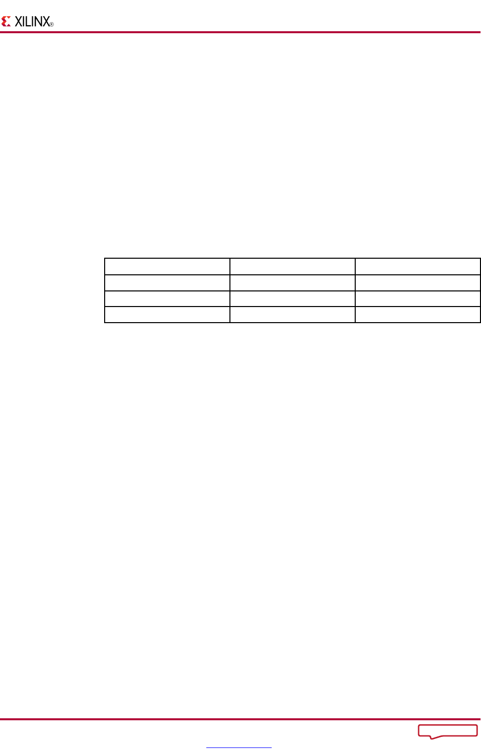
Criteria for Implementing Inferred RAM on Block RAM Resources
Devices
Depth
Depth * Width
Spartan®-6
>= 127 words > 512 bits
Virtex®-6
>= 127 words > 512 bits
7 series
>= 127 words > 512 bits
Implementing General Logic and FSM Components on Block RAM
• XST can implement the following on block RAM resources:
– General logic
– FSM Components
• For more information, see Mapping Logic to Block RAM.
Block RAM Resource Management
• XST takes into account the actual amount of block RAM resources available in order
to avoid overmapping the device.
– XST may use all available block RAM resources.
– BRAM Utilization Ratio forces XST to leave some block RAM resources
unallocated.
• XST determines the actual amount of block RAM resources available for inferred
RAM macros. XST subtracts the following amounts from the overall pool
theoretically dened by BRAM Utilization Ratio:
1. Block RAM that you have instantiated.
2. RAM and ROM components that you forced to block RAM implementation with
RAM Style or ROM Style. XST honors those constraints before attempting to
implement other inferred RAM components to block resources.
3. Block RAM resulting from the mapping of logic or Finite State Machine (FSM)
components to Map Logic on BRAM.
• The XST block RAM allocation strategy favors the largest inferred RAM components
for block implementation. This strategy allows smaller RAM components to go to
block resources if there are any left on the device.
• Block RAM over-utilization can occur if the sum of block RAM components created
from the three cases listed above exceeds available resources. XST avoids this
over-utilization in most cases.
XST User Guide for Virtex-6, Spartan-6, and 7 Series Devices
UG687 (v 14.5) March 20, 2013 www.xilinx.com 239
Send Feedback

Chapter 7: HDL Coding Techniques
Block RAM Packing
• XST can implement additional RAM on block resources by packing small single-port
RAM components together.
• XST can implement two single-port RAM components on a single dual-port block
RAM primitive. Each port manages a physically distinct part of the block RAM.
• This optimization is controlled by Automatic BRAM Packing, and is disabled by
default.
Distributed RAM Pipelining
• XST can pipeline RAM components implemented on distributed resources.
– There must be an adequate number of latency stages.
– The effect of pipelining is similar to Flip-Flop Retiming.
– The result is increased performance.
• To insert pipeline stages:
1. Describe the necessary number of Registers in the HDL source code.
2. Place the Registers after the RAM.
3. Set RAM Style to pipe_distributed.
• During pipelining:
– XST calculates the ideal number of Register stages needed to maximize
operating frequency.
– XST issues an HDL Advisor message if there are fewer than the ideal number of
Register stages. The message reports the number of additional Register stages
needed to achieve the ideal number.
– XST cannot pipeline distributed RAM components if the Registers have
asynchronous set or reset logic.
– XST can pipeline RAM components if Registers contain synchronous reset
signals.
RAM Related Constraints
• The RAM related constraints are:
– RAM Extraction
– RAM Style
– ROM Extraction
– ROM Style
– BRAM Utilization Ratio
– Automatic BRAM Packing
• XST accepts LOC and RLOC on inferred RAM implemented in a single block RAM
primitive.
• LOC and RLOC are propagated to the NGC netlist.
XST User Guide for Virtex-6, Spartan-6, and 7 Series Devices
240 www.xilinx.com UG687 (v 14.5) March 20, 2013
Send Feedback

Chapter 7: HDL Coding Techniques
RAM Reporting
• XST provides detailed information on inferred RAM, including:
– Size
– Synchronization
– Control signals
• RAM recognition consists of two steps:
1. HDL Synthesis
XST recognizes the presence of the memory structure in the HDL source code.
2. Advanced HDL Synthesis
After acquiring a more accurate picture of each RAM component, XST
implements them on distributed or block RAM resources, depending on
resource availability.
• An inferred block RAM is generally reported as shown in the following example.
XST User Guide for Virtex-6, Spartan-6, and 7 Series Devices
UG687 (v 14.5) March 20, 2013 www.xilinx.com 241
Send Feedback

Chapter 7: HDL Coding Techniques
RAM Reporting Log Example
=========================================================================
* HDL Synthesis *
=========================================================================
Synthesizing Unit <rams_27>.
Found 16-bit register for signal <do>.
Found 128x16-bit dual-port <RAM Mram_RAM> for signal <RAM>.
Summary:
inferred 1 RAM(s).
inferred 16 D-type flip-flop(s).
Unit <rams_27> synthesized.
=========================================================================
HDL Synthesis Report
Macro Statistics
# RAMs : 1
128x16-bit dual-port RAM : 1
# Registers : 1
16-bit register : 1
=========================================================================
=========================================================================
* Advanced HDL Synthesis *
=========================================================================
Synthesizing (advanced) Unit <rams_27>.
INFO:Xst - The <RAM Mram_RAM> will be implemented as a BLOCK RAM,
absorbing the following register(s): <do>
-----------------------------------------------------------------------
| ram_type | Block | |
-----------------------------------------------------------------------
| Port A |
| aspect ratio | 128-word x 16-bit | |
| mode | read-first | |
| clkA | connected to signal <clk> | rise |
| weA | connected to signal <we> | high |
| addrA | connected to signal <waddr> | |
| diA | connected to signal <di> | |
-----------------------------------------------------------------------
| optimization | speed | |
-----------------------------------------------------------------------
| Port B |
| aspect ratio | 128-word x 16-bit | |
| mode | write-first | |
| clkB | connected to signal <clk> | rise |
| enB | connected to signal <re> | high |
| addrB | connected to signal <raddr> | |
| doB | connected to signal <do> | |
-----------------------------------------------------------------------
| optimization | speed | |
-----------------------------------------------------------------------
Unit <rams_27> synthesized (advanced).
=========================================================================
Advanced HDL Synthesis Report
Macro Statistics
# RAMs : 1
128x16-bit dual-port block RAM : 1
=========================================================================
XST User Guide for Virtex-6, Spartan-6, and 7 Series Devices
242 www.xilinx.com UG687 (v 14.5) March 20, 2013
Send Feedback

Chapter 7: HDL Coding Techniques
Pipelining of Distributed RAM Reporting Log Example
Pipelining of a distributed RAM results in the following specic reporting in the
Advanced HDL Synthesis section.
Synthesizing (advanced) Unit <v_rams_22>.
Found pipelined ram on signal <n0006>:
- 1 pipeline level(s) found in a register on signal <n0006>.
Pushing register(s) into the ram macro.
INFO:Xst:2390 - HDL ADVISOR - You can improve the performance of the ram Mram_RAM
by adding 1 register level(s) on output signal n0006.
Unit <v_rams_22> synthesized (advanced).
RAM Coding Examples
For update information, see “Coding Examples” in the Introduction.
Single-Port RAM with Asynchronous Read (Distributed RAM) VHDL Coding
Example
--
-- Single-Port RAM with Asynchronous Read (Distributed RAM)
--
-- Download: http://www.xilinx.com/txpatches/pub/documentation/misc/xstug_examples.zip
-- File: HDL_Coding_Techniques/rams/rams_04.vhd
--
library ieee;
use ieee.std_logic_1164.all;
use ieee.std_logic_unsigned.all;
entity rams_04 is
port (clk : in std_logic;
we : in std_logic;
a : in std_logic_vector(5 downto 0);
di : in std_logic_vector(15 downto 0);
do : out std_logic_vector(15 downto 0));
end rams_04;
architecture syn of rams_04 is
type ram_type is array (63 downto 0) of std_logic_vector (15 downto 0);
signal RAM : ram_type;
begin
process (clk)
begin
if (clk’event and clk = ’1’) then
if (we = ’1’) then
RAM(conv_integer(a)) <= di;
end if;
end if;
end process;
do <= RAM(conv_integer(a));
end syn;
XST User Guide for Virtex-6, Spartan-6, and 7 Series Devices
UG687 (v 14.5) March 20, 2013 www.xilinx.com 243
Send Feedback

Chapter 7: HDL Coding Techniques
Dual-Port RAM with Asynchronous Read (Distributed RAM) Verilog Coding
Example
//
// Dual-Port RAM with Asynchronous Read (Distributed RAM)
//
// Download: http://www.xilinx.com/txpatches/pub/documentation/misc/xstug_examples.zip
// File: HDL_Coding_Techniques/rams/rams_09.v
//
module v_rams_09 (clk, we, a, dpra, di, spo, dpo);
input clk;
input we;
input [5:0] a;
input [5:0] dpra;
input [15:0] di;
output [15:0] spo;
output [15:0] dpo;
reg [15:0] ram [63:0];
always @(posedge clk) begin
if (we)
ram[a] <= di;
end
assign spo = ram[a];
assign dpo = ram[dpra];
endmodule
Single-Port Block RAM Read-First Mode VHDL Coding Example
--
-- Single-Port Block RAM Read-First Mode
--
-- Download: http://www.xilinx.com/txpatches/pub/documentation/misc/xstug_examples.zip
-- File: HDL_Coding_Techniques/rams/rams_01.vhd
--
library ieee;
use ieee.std_logic_1164.all;
use ieee.std_logic_unsigned.all;
entity rams_01 is
port (clk : in std_logic;
we : in std_logic;
en : in std_logic;
addr : in std_logic_vector(5 downto 0);
di : in std_logic_vector(15 downto 0);
do : out std_logic_vector(15 downto 0));
end rams_01;
architecture syn of rams_01 is
type ram_type is array (63 downto 0) of std_logic_vector (15 downto 0);
signal RAM: ram_type;
begin
process (clk)
begin
if clk’event and clk = ’1’ then
if en = ’1’ then
if we = ’1’ then
RAM(conv_integer(addr)) <= di;
end if;
do <= RAM(conv_integer(addr)) ;
end if;
end if;
end process;
end syn;
XST User Guide for Virtex-6, Spartan-6, and 7 Series Devices
244 www.xilinx.com UG687 (v 14.5) March 20, 2013
Send Feedback

Chapter 7: HDL Coding Techniques
Single-Port Block RAM Read-First Mode Verilog Coding Example
//
// Single-Port Block RAM Read-First Mode
//
// Download: http://www.xilinx.com/txpatches/pub/documentation/misc/xstug_examples.zip
// File: HDL_Coding_Techniques/rams/rams_01.v
//
module v_rams_01 (clk, en, we, addr, di, do);
input clk;
input we;
input en;
input [5:0] addr;
input [15:0] di;
output [15:0] do;
reg [15:0] RAM [63:0];
reg [15:0] do;
always @(posedge clk)
begin
if (en)
begin
if (we)
RAM[addr]<=di;
do <= RAM[addr];
end
end
endmodule
XST User Guide for Virtex-6, Spartan-6, and 7 Series Devices
UG687 (v 14.5) March 20, 2013 www.xilinx.com 245
Send Feedback

Chapter 7: HDL Coding Techniques
Single-Port Block RAM Write-First Mode VHDL Coding Example
--
-- Single-Port Block RAM Write-First Mode (recommended template)
--
-- Download: http://www.xilinx.com/txpatches/pub/documentation/misc/xstug_examples.zip
-- File: HDL_Coding_Techniques/rams/rams_02a.vhd
--
library ieee;
use ieee.std_logic_1164.all;
use ieee.std_logic_unsigned.all;
entity rams_02a is
port (clk : in std_logic;
we : in std_logic;
en : in std_logic;
addr : in std_logic_vector(5 downto 0);
di : in std_logic_vector(15 downto 0);
do : out std_logic_vector(15 downto 0));
end rams_02a;
architecture syn of rams_02a is
type ram_type is array (63 downto 0)
of std_logic_vector (15 downto 0);
signal RAM : ram_type;
begin
process (clk)
begin
if clk’event and clk = ’1’ then
if en = ’1’ then
if we = ’1’ then
RAM(conv_integer(addr)) <= di;
do <= di;
else
do <= RAM( conv_integer(addr));
end if;
end if;
end if;
end process;
end syn;
XST User Guide for Virtex-6, Spartan-6, and 7 Series Devices
246 www.xilinx.com UG687 (v 14.5) March 20, 2013
Send Feedback

Chapter 7: HDL Coding Techniques
Single-Port Block RAM Write-First Mode Verilog Coding Example
//
// Single-Port Block RAM Write-First Mode (recommended template)
//
// Download: http://www.xilinx.com/txpatches/pub/documentation/misc/xstug_examples.zip
// File: HDL_Coding_Techniques/rams/rams_02a.v
//
module v_rams_02a (clk, we, en, addr, di, do);
input clk;
input we;
input en;
input [5:0] addr;
input [15:0] di;
output [15:0] do;
reg [15:0] RAM [63:0];
reg [15:0] do;
always @(posedge clk)
begin
if (en)
begin
if (we)
begin
RAM[addr] <= di;
do <= di;
end
else
do <= RAM[addr];
end
end
endmodule
XST User Guide for Virtex-6, Spartan-6, and 7 Series Devices
UG687 (v 14.5) March 20, 2013 www.xilinx.com 247
Send Feedback

Chapter 7: HDL Coding Techniques
Single-Port Block RAM No-Change Mode VHDL Coding Example
--
-- Single-Port Block RAM No-Change Mode
--
-- Download: http://www.xilinx.com/txpatches/pub/documentation/misc/xstug_examples.zip
-- File: HDL_Coding_Techniques/rams/rams_03.vhd
--
library ieee;
use ieee.std_logic_1164.all;
use ieee.std_logic_unsigned.all;
entity rams_03 is
port (clk : in std_logic;
we : in std_logic;
en : in std_logic;
addr : in std_logic_vector(5 downto 0);
di : in std_logic_vector(15 downto 0);
do : out std_logic_vector(15 downto 0));
end rams_03;
architecture syn of rams_03 is
type ram_type is array (63 downto 0) of std_logic_vector (15 downto 0);
signal RAM : ram_type;
begin
process (clk)
begin
if clk’event and clk = ’1’ then
if en = ’1’ then
if we = ’1’ then
RAM(conv_integer(addr)) <= di;
else
do <= RAM( conv_integer(addr));
end if;
end if;
end if;
end process;
end syn;
XST User Guide for Virtex-6, Spartan-6, and 7 Series Devices
248 www.xilinx.com UG687 (v 14.5) March 20, 2013
Send Feedback

Chapter 7: HDL Coding Techniques
Single-Port Block RAM No-Change Mode Verilog Coding Example
//
// Single-Port Block RAM No-Change Mode
//
// Download: http://www.xilinx.com/txpatches/pub/documentation/misc/xstug_examples.zip
// File: HDL_Coding_Techniques/rams/rams_03.v
//
module v_rams_03 (clk, we, en, addr, di, do);
input clk;
input we;
input en;
input [5:0] addr;
input [15:0] di;
output [15:0] do;
reg [15:0] RAM [63:0];
reg [15:0] do;
always @(posedge clk)
begin
if (en)
begin
if (we)
RAM[addr] <= di;
else
do <= RAM[addr];
end
end
endmodule
XST User Guide for Virtex-6, Spartan-6, and 7 Series Devices
UG687 (v 14.5) March 20, 2013 www.xilinx.com 249
Send Feedback

Chapter 7: HDL Coding Techniques
Dual-Port Block RAM with Two Write Ports VHDL Coding Example
--
-- Dual-Port Block RAM with Two Write Ports
-- Correct Modelization with a Shared Variable
--
-- Download: http://www.xilinx.com/txpatches/pub/documentation/misc/xstug_examples.zip
-- File: HDL_Coding_Techniques/rams/rams_16b.vhd
--
library IEEE;
use IEEE.std_logic_1164.all;
use IEEE.std_logic_unsigned.all;
entity rams_16b is
port(clka : in std_logic;
clkb : in std_logic;
ena : in std_logic;
enb : in std_logic;
wea : in std_logic;
web : in std_logic;
addra : in std_logic_vector(6 downto 0);
addrb : in std_logic_vector(6 downto 0);
dia : in std_logic_vector(15 downto 0);
dib : in std_logic_vector(15 downto 0);
doa : out std_logic_vector(15 downto 0);
dob : out std_logic_vector(15 downto 0));
end rams_16b;
architecture syn of rams_16b is
type ram_type is array (127 downto 0) of std_logic_vector(15 downto 0);
shared variable RAM : ram_type;
begin
process (CLKA)
begin
if CLKA’event and CLKA = ’1’ then
if ENA = ’1’ then
DOA <= RAM(conv_integer(ADDRA));
if WEA = ’1’ then
RAM(conv_integer(ADDRA)) := DIA;
end if;
end if;
end if;
end process;
process (CLKB)
begin
if CLKB’event and CLKB = ’1’ then
if ENB = ’1’ then
DOB <= RAM(conv_integer(ADDRB));
if WEB = ’1’ then
RAM(conv_integer(ADDRB)) := DIB;
end if;
end if;
end if;
end process;
end syn;
XST User Guide for Virtex-6, Spartan-6, and 7 Series Devices
250 www.xilinx.com UG687 (v 14.5) March 20, 2013
Send Feedback

Chapter 7: HDL Coding Techniques
Dual-Port Block RAM with Two Write Ports Verilog Coding Example
//
// Dual-Port Block RAM with Two Write Ports
//
// Download: http://www.xilinx.com/txpatches/pub/documentation/misc/xstug_examples.zip
// File: HDL_Coding_Techniques/rams/rams_16.v
//
module v_rams_16 (clka,clkb,ena,enb,wea,web,addra,addrb,dia,dib,doa,dob);
input clka,clkb,ena,enb,wea,web;
input [5:0] addra,addrb;
input [15:0] dia,dib;
output [15:0] doa,dob;
reg [15:0] ram [63:0];
reg [15:0] doa,dob;
always @(posedge clka) begin
if (ena)
begin
if (wea)
ram[addra] <= dia;
doa <= ram[addra];
end
end
always @(posedge clkb) begin
if (enb)
begin
if (web)
ram[addrb] <= dib;
dob <= ram[addrb];
end
end
endmodule
XST User Guide for Virtex-6, Spartan-6, and 7 Series Devices
UG687 (v 14.5) March 20, 2013 www.xilinx.com 251
Send Feedback

Chapter 7: HDL Coding Techniques
Block RAM with Resettable Data Output VHDL Coding Example
--
-- Block RAM with Resettable Data Output
--
-- Download: http://www.xilinx.com/txpatches/pub/documentation/misc/xstug_examples.zip
-- File: HDL_Coding_Techniques/rams/rams_18.vhd
--
library ieee;
use ieee.std_logic_1164.all;
use ieee.std_logic_unsigned.all;
entity rams_18 is
port (clk : in std_logic;
en : in std_logic;
we : in std_logic;
rst : in std_logic;
addr : in std_logic_vector(6 downto 0);
di : in std_logic_vector(15 downto 0);
do : out std_logic_vector(15 downto 0));
end rams_18;
architecture syn of rams_18 is
type ram_type is array (127 downto 0) of std_logic_vector (15 downto 0);
signal ram : ram_type;
begin
process (clk)
begin
if clk’event and clk = ’1’ then
if en = ’1’ then -- optional enable
if we = ’1’ then -- write enable
ram(conv_integer(addr)) <= di;
end if;
if rst = ’1’ then -- optional reset
do <= (others => ’0’);
else
do <= ram(conv_integer(addr));
end if;
end if;
end if;
end process;
end syn;
XST User Guide for Virtex-6, Spartan-6, and 7 Series Devices
252 www.xilinx.com UG687 (v 14.5) March 20, 2013
Send Feedback

Chapter 7: HDL Coding Techniques
Block RAM with Resettable Data Output Verilog Coding Example
//
// Block RAM with Resettable Data Output
//
// Download: http://www.xilinx.com/txpatches/pub/documentation/misc/xstug_examples.zip
// File: HDL_Coding_Techniques/rams/rams_18.v
//
module v_rams_18 (clk, en, we, rst, addr, di, do);
input clk;
input en;
input we;
input rst;
input [6:0] addr;
input [15:0] di;
output [15:0] do;
reg [15:0] ram [127:0];
reg [15:0] do;
always @(posedge clk)
begin
if (en) // optional enable
begin
if (we) // write enable
ram[addr] <= di;
if (rst) // optional reset
do <= 16’b0000111100001101;
else
do <= ram[addr];
end
end
endmodule
XST User Guide for Virtex-6, Spartan-6, and 7 Series Devices
UG687 (v 14.5) March 20, 2013 www.xilinx.com 253
Send Feedback

Chapter 7: HDL Coding Techniques
Block RAM with Optional Output Registers VHDL Coding Example
--
-- Block RAM with Optional Output Registers
--
-- Download: http://www.xilinx.com/txpatches/pub/documentation/misc/xstug_examples.zip
-- File: HDL_Coding_Techniques/rams/rams_19.vhd
--
library IEEE;
library IEEE;
use IEEE.STD_LOGIC_1164.ALL;
use IEEE.STD_LOGIC_UNSIGNED.ALL;
entity rams_19 is
port (clk1, clk2 : in std_logic;
we, en1, en2 : in std_logic;
addr1 : in std_logic_vector(5 downto 0);
addr2 : in std_logic_vector(5 downto 0);
di : in std_logic_vector(15 downto 0);
res1 : out std_logic_vector(15 downto 0);
res2 : out std_logic_vector(15 downto 0));
end rams_19;
architecture beh of rams_19 is
type ram_type is array (63 downto 0) of std_logic_vector (15 downto 0);
signal ram : ram_type;
signal do1 : std_logic_vector(15 downto 0);
signal do2 : std_logic_vector(15 downto 0);
begin
process (clk1)
begin
if rising_edge(clk1) then
if we = ’1’ then
ram(conv_integer(addr1)) <= di;
end if;
do1 <= ram(conv_integer(addr1));
end if;
end process;
process (clk2)
begin
if rising_edge(clk2) then
do2 <= ram(conv_integer(addr2));
end if;
end process;
process (clk1)
begin
if rising_edge(clk1) then
if en1 = ’1’ then
res1 <= do1;
end if;
end if;
end process;
process (clk2)
begin
if rising_edge(clk2) then
if en2 = ’1’ then
res2 <= do2;
end if;
end if;
end process;
end beh;
XST User Guide for Virtex-6, Spartan-6, and 7 Series Devices
254 www.xilinx.com UG687 (v 14.5) March 20, 2013
Send Feedback

Chapter 7: HDL Coding Techniques
Block RAM with Optional Output Registers Verilog Coding Example
//
// Block RAM with Optional Output Registers
//
// Download: http://www.xilinx.com/txpatches/pub/documentation/misc/xstug_examples.zip
// File: HDL_Coding_Techniques/rams/rams_19.v
//
module v_rams_19 (clk1, clk2, we, en1, en2, addr1, addr2, di, res1, res2);
input clk1;
input clk2;
input we, en1, en2;
input [6:0] addr1;
input [6:0] addr2;
input [15:0] di;
output [15:0] res1;
output [15:0] res2;
reg [15:0] res1;
reg [15:0] res2;
reg [15:0] RAM [127:0];
reg [15:0] do1;
reg [15:0] do2;
always @(posedge clk1)
begin
if (we == 1’b1)
RAM[addr1] <= di;
do1 <= RAM[addr1];
end
always @(posedge clk2)
begin
do2 <= RAM[addr2];
end
always @(posedge clk1)
begin
if (en1 == 1’b1)
res1 <= do1;
end
always @(posedge clk2)
begin
if (en2 == 1’b1)
res2 <= do2;
end
endmodule
XST User Guide for Virtex-6, Spartan-6, and 7 Series Devices
UG687 (v 14.5) March 20, 2013 www.xilinx.com 255
Send Feedback

Chapter 7: HDL Coding Techniques
Initializing Block RAM (Single-Por t Block RAM) VHDL Coding Example
--
-- Initializing Block RAM (Single-Port Block RAM)
--
-- Download: http://www.xilinx.com/txpatches/pub/documentation/misc/xstug_examples.zip
-- File: HDL_Coding_Techniques/rams/rams_20a.vhd
--
library ieee;
use ieee.std_logic_1164.all;
use ieee.std_logic_unsigned.all;
entity rams_20a is
port (clk : in std_logic;
we : in std_logic;
addr : in std_logic_vector(5 downto 0);
di : in std_logic_vector(19 downto 0);
do : out std_logic_vector(19 downto 0));
end rams_20a;
architecture syn of rams_20a is
type ram_type is array (63 downto 0) of std_logic_vector (19 downto 0);
signal RAM : ram_type:= (X"0200A", X"00300", X"08101", X"04000", X"08601", X"0233A",
X"00300", X"08602", X"02310", X"0203B", X"08300", X"04002",
X"08201", X"00500", X"04001", X"02500", X"00340", X"00241",
X"04002", X"08300", X"08201", X"00500", X"08101", X"00602",
X"04003", X"0241E", X"00301", X"00102", X"02122", X"02021",
X"00301", X"00102", X"02222", X"04001", X"00342", X"0232B",
X"00900", X"00302", X"00102", X"04002", X"00900", X"08201",
X"02023", X"00303", X"02433", X"00301", X"04004", X"00301",
X"00102", X"02137", X"02036", X"00301", X"00102", X"02237",
X"04004", X"00304", X"04040", X"02500", X"02500", X"02500",
X"0030D", X"02341", X"08201", X"0400D");
begin
process (clk)
begin
if rising_edge(clk) then
if we = ’1’ then
RAM(conv_integer(addr)) <= di;
end if;
do <= RAM(conv_integer(addr));
end if;
end process;
end syn;
XST User Guide for Virtex-6, Spartan-6, and 7 Series Devices
256 www.xilinx.com UG687 (v 14.5) March 20, 2013
Send Feedback

Chapter 7: HDL Coding Techniques
Initializing Block RAM (Single-Port Block RAM) Verilog Coding Example
//
// Initializing Block RAM (Single-Port Block RAM)
//
// Download: http://www.xilinx.com/txpatches/pub/documentation/misc/xstug_examples.zip
// File: HDL_Coding_Techniques/rams/rams_20a.v
//
module v_rams_20a (clk, we, addr, di, do);
input clk;
input we;
input [5:0] addr;
input [19:0] di;
output [19:0] do;
reg [19:0] ram [63:0];
reg [19:0] do;
initial begin
ram[63] = 20’h0200A; ram[62] = 20’h00300; ram[61] = 20’h08101;
ram[60] = 20’h04000; ram[59] = 20’h08601; ram[58] = 20’h0233A;
ram[57] = 20’h00300; ram[56] = 20’h08602; ram[55] = 20’h02310;
ram[54] = 20’h0203B; ram[53] = 20’h08300; ram[52] = 20’h04002;
ram[51] = 20’h08201; ram[50] = 20’h00500; ram[49] = 20’h04001;
ram[48] = 20’h02500; ram[47] = 20’h00340; ram[46] = 20’h00241;
ram[45] = 20’h04002; ram[44] = 20’h08300; ram[43] = 20’h08201;
ram[42] = 20’h00500; ram[41] = 20’h08101; ram[40] = 20’h00602;
ram[39] = 20’h04003; ram[38] = 20’h0241E; ram[37] = 20’h00301;
ram[36] = 20’h00102; ram[35] = 20’h02122; ram[34] = 20’h02021;
ram[33] = 20’h00301; ram[32] = 20’h00102; ram[31] = 20’h02222;
ram[30] = 20’h04001; ram[29] = 20’h00342; ram[28] = 20’h0232B;
ram[27] = 20’h00900; ram[26] = 20’h00302; ram[25] = 20’h00102;
ram[24] = 20’h04002; ram[23] = 20’h00900; ram[22] = 20’h08201;
ram[21] = 20’h02023; ram[20] = 20’h00303; ram[19] = 20’h02433;
ram[18] = 20’h00301; ram[17] = 20’h04004; ram[16] = 20’h00301;
ram[15] = 20’h00102; ram[14] = 20’h02137; ram[13] = 20’h02036;
ram[12] = 20’h00301; ram[11] = 20’h00102; ram[10] = 20’h02237;
ram[9] = 20’h04004; ram[8] = 20’h00304; ram[7] = 20’h04040;
ram[6] = 20’h02500; ram[5] = 20’h02500; ram[4] = 20’h02500;
ram[3] = 20’h0030D; ram[2] = 20’h02341; ram[1] = 20’h08201;
ram[0] = 20’h0400D;
end
always @(posedge clk)
begin
if (we)
ram[addr] <= di;
do <= ram[addr];
end
endmodule
XST User Guide for Virtex-6, Spartan-6, and 7 Series Devices
UG687 (v 14.5) March 20, 2013 www.xilinx.com 257
Send Feedback

Chapter 7: HDL Coding Techniques
Initializing Block RAM From an External Data File VHDL Coding Example
--
-- Initializing Block RAM from external data file
--
-- Download: http://www.xilinx.com/txpatches/pub/documentation/misc/xstug_examples.zip
-- File: HDL_Coding_Techniques/rams/rams_20c.vhd
--
library ieee;
use ieee.std_logic_1164.all;
use ieee.std_logic_unsigned.all;
use std.textio.all;
entity rams_20c is
port(clk : in std_logic;
we : in std_logic;
addr : in std_logic_vector(5 downto 0);
din : in std_logic_vector(31 downto 0);
dout : out std_logic_vector(31 downto 0));
end rams_20c;
architecture syn of rams_20c is
type RamType is array(0 to 63) of bit_vector(31 downto 0);
impure function InitRamFromFile (RamFileName : in string) return RamType is
FILE RamFile : text is in RamFileName;
variable RamFileLine : line;
variable RAM : RamType;
begin
for I in RamType’range loop
readline (RamFile, RamFileLine);
read (RamFileLine, RAM(I));
end loop;
return RAM;
end function;
signal RAM : RamType := InitRamFromFile("rams_20c.data");
begin
process (clk)
begin
if clk’event and clk = ’1’ then
if we = ’1’ then
RAM(conv_integer(addr)) <= to_bitvector(din);
end if;
dout <= to_stdlogicvector(RAM(conv_integer(addr)));
end if;
end process;
end syn;
XST User Guide for Virtex-6, Spartan-6, and 7 Series Devices
258 www.xilinx.com UG687 (v 14.5) March 20, 2013
Send Feedback

Chapter 7: HDL Coding Techniques
Initializing Block RAM From an External Data File Verilog Coding Example
//
// Initializing Block RAM from external data file
// Binary data
//
// Download: http://www.xilinx.com/txpatches/pub/documentation/misc/xstug_examples.zip
// File: HDL_Coding_Techniques/rams/rams_20c.v
//
module v_rams_20c (clk, we, addr, din, dout);
input clk;
input we;
input [5:0] addr;
input [31:0] din;
output [31:0] dout;
reg [31:0] ram [0:63];
reg [31:0] dout;
initial
begin
// $readmemb("rams_20c.data",ram, 0, 63);
$readmemb("rams_20c.data",ram);
end
always @(posedge clk)
begin
if (we)
ram[addr] <= din;
dout <= ram[addr];
end
endmodule
XST User Guide for Virtex-6, Spartan-6, and 7 Series Devices
UG687 (v 14.5) March 20, 2013 www.xilinx.com 259
Send Feedback

Chapter 7: HDL Coding Techniques
Pipelined Distributed RAM VHDL Coding Example
--
-- Pipeline distributed RAM
--
-- Download: http://www.xilinx.com/txpatches/pub/documentation/misc/xstug_examples.zip
-- File: HDL_Coding_Techniques/rams/rams_22.vhd
--
library ieee;
use ieee.std_logic_1164.all;
use ieee.std_logic_unsigned.all;
entity rams_22 is
port (clk : in std_logic;
we : in std_logic;
addr : in std_logic_vector(8 downto 0);
di : in std_logic_vector(3 downto 0);
do : out std_logic_vector(3 downto 0));
end rams_22;
architecture syn of rams_22 is
type ram_type is array (511 downto 0) of std_logic_vector (3 downto 0);
signal RAM : ram_type;
signal pipe_reg: std_logic_vector(3 downto 0);
attribute ram_style: string;
attribute ram_style of RAM: signal is "pipe_distributed";
begin
process (clk)
begin
if clk’event and clk = ’1’ then
if we = ’1’ then
RAM(conv_integer(addr)) <= di;
else
pipe_reg <= RAM( conv_integer(addr));
end if;
do <= pipe_reg;
end if;
end process;
end syn;
XST User Guide for Virtex-6, Spartan-6, and 7 Series Devices
260 www.xilinx.com UG687 (v 14.5) March 20, 2013
Send Feedback

Chapter 7: HDL Coding Techniques
Pipelined Distributed RAM Verilog Coding Example
//
// Pipeline distributed RAM
//
// Download: http://www.xilinx.com/txpatches/pub/documentation/misc/xstug_examples.zip
// File: HDL_Coding_Techniques/rams/rams_22.v
//
module v_rams_22 (clk, we, addr, di, do);
input clk;
input we;
input [8:0] addr;
input [3:0] di;
output [3:0] do;
(*ram_style="pipe_distributed"*)
reg [3:0] RAM [511:0];
reg [3:0] do;
reg [3:0] pipe_reg;
always @(posedge clk)
begin
if (we)
RAM[addr] <= di;
else
pipe_reg <= RAM[addr];
do <= pipe_reg;
end
endmodule
XST User Guide for Virtex-6, Spartan-6, and 7 Series Devices
UG687 (v 14.5) March 20, 2013 www.xilinx.com 261
Send Feedback

Chapter 7: HDL Coding Techniques
ROM HDL Coding Techniques
Read-Only Memory (ROM) closely resembles Random Access Memory (RAM) with
respect to HDL modeling and implementation. XST can implement a properly-registered
ROM on block RAM resources.
ROM Description
ROM Description includes:
• ROM Modeling
• Describing Read Access
ROM Modeling
ROM Modeling includes:
• Loading ROM From an External Data File
• ROM Modeling in VHDL
• ROM Modeling in Verilog
Loading ROM From an External Data File
• Loading the content of the ROM from an external data le:
– Results in more compact and readable HDL source code.
– Allows more exibility in generating or altering the ROM data.
• For more information, see Specifying RAM Initial Contents in an External Data File.
ROM Modeling in VHDL
For ROM modeling in VHDL:
• Use a signal.
A signal allows you to control implementation of the ROM, either on:
– LUT resources, or
– block RAM resources
• Attach a ROM Style or a RAM Style constraint to the signal to control
implementation of the ROM.
Constant-Based Declaration VHDL Coding Example
type rom_type is array (0 to 127) of std_logic_vector (19 downto 0);
constant ROM : rom_type:= (
X"0200A", X"00300", X"08101", X"04000", X"08601", X"0233A", X"00300", X"08602",
X"02310", X"0203B", X"08300", X"04002", X"08201", X"00500", X"04001", X"02500",
(…)
X"04078", X"01110", X"02500", X"02500", X"0030D", X"02341", X"08201", X"0410D"
);
Signal-Based Declaration VHDL Coding Example
type rom_type is array (0 to 127) of std_logic_vector (19 downto 0);
signal ROM : rom_type:= (
X"0200A", X"00300", X"08101", X"04000", X"08601", X"0233A", X"00300", X"08602",
X"02310", X"0203B", X"08300", X"04002", X"08201", X"00500", X"04001", X"02500",
(…)
X"04078", X"01110", X"02500", X"02500", X"0030D", X"02341", X"08201", X"0410D"
);
XST User Guide for Virtex-6, Spartan-6, and 7 Series Devices
262 www.xilinx.com UG687 (v 14.5) March 20, 2013
Send Feedback

Chapter 7: HDL Coding Techniques
ROM Modeling in Verilog
• A ROM can be modeled in Verilog with an initial block.
• Verilog does not allow initializing an array with a single statement as allowed by
VHDL aggregates.
• You must enumerate each address value.
ROM Modeled With Initial Block Verilog Coding Example
reg [15:0] rom [15:0];
initial begin
rom[0] = 16’b0011111100000010;
rom[1] = 16’b0000000100001001;
rom[2] = 16’b0001000000111000;
rom[3] = 16’b0000000000000000;
rom[4] = 16’b1100001010011000;
rom[5] = 16’b0000000000000000;
rom[6] = 16’b0000000110000000;
rom[7] = 16’b0111111111110000;
rom[8] = 16’b0010000010001001;
rom[9] = 16’b0101010101011000;
rom[10] = 16’b1111111010101010;
rom[11] = 16’b0000000000000000;
rom[12] = 16’b1110000000001000;
rom[13] = 16’b0000000110001010;
rom[14] = 16’b0110011100010000;
rom[15] = 16’b0000100010000000;
end
Describing ROM With a Case Statement Verilog Coding Example
You can also describe the ROM with a case statement (or equivalent if-elseif construct).
input [3:0] addr
output reg [15:0] data;
always @(posedge clk) begin
if (en)
case (addr)
4’b0000: data <= 16’h200A;
4’b0001: data <= 16’h0300;
4’b0010: data <= 16’h8101;
4’b0011: data <= 16’h4000;
4’b0100: data <= 16’h8601;
4’b0101: data <= 16’h233A;
4’b0110: data <= 16’h0300;
4’b0111: data <= 16’h8602;
4’b1000: data <= 16’h2222;
4’b1001: data <= 16’h4001;
4’b1010: data <= 16’h0342;
4’b1011: data <= 16’h232B;
4’b1100: data <= 16’h0900;
4’b1101: data <= 16’h0302;
4’b1110: data <= 16’h0102;
4’b1111: data <= 16’h4002;
endcase
end
XST User Guide for Virtex-6, Spartan-6, and 7 Series Devices
UG687 (v 14.5) March 20, 2013 www.xilinx.com 263
Send Feedback

Chapter 7: HDL Coding Techniques
Describing Read Access
Describing access to ROM is similar to describing access to RAM.
Describing Read Access VHDL Coding Example
If you have included the IEEE std_logic_unsigned package dening the conv_integer
conversion function, the VHDL syntax is:
signal addr : std_logic_vector(ADDR_WIDTH-1 downto 0);
do <= ROM( conv_integer(addr));
Describing Read Access Verilog Coding Example
• If you have modeled the ROM in an initial block (with data described in the Verilog
source code or loaded from an external data le), the Verilog syntax is:
do <= ROM[addr];
• You can also use a case construct as shown in Describing ROM With a Case
Statement Verilog Coding Example.
ROM Implementation
• When XST detects that a properly synchronized ROM can be implemented on block
RAM resources, it applies the principles outlined in Block RAM Optimization
Strategies.
• To override any default XST decision criteria, use ROM Style instead of RAM Style.
• For more information about ROM Style, see Chapter 9, Design Constraints.
• For more information about ROM implementation, see Chapter 8, FPGA
Optimization.
ROM Related Constraints
ROM Style
ROM Reporting
The following report shows how the Read-Only Memory (ROM) is identied during
HDL Synthesis. Based on the availability of proper synchronization, the decision to
implement a ROM on block RAM resources is made during Advanced HDL Synthesis.
XST User Guide for Virtex-6, Spartan-6, and 7 Series Devices
264 www.xilinx.com UG687 (v 14.5) March 20, 2013
Send Feedback

Chapter 7: HDL Coding Techniques
ROM Repor ting Example
=========================================================================
* HDL Synthesis *
=========================================================================
Synthesizing Unit <roms_signal>.
Found 20-bit register for signal <data>.
Found 128x20-bit ROM for signal <n0024>.
Summary:
inferred 1 ROM(s).
inferred 20 D-type flip-flop(s).
Unit <roms_signal> synthesized.
=========================================================================
HDL Synthesis Report
Macro Statistics
# ROMs : 1
128x20-bit ROM : 1
# Registers : 1
20-bit register : 1
=========================================================================
=========================================================================
* Advanced HDL Synthesis *
=========================================================================
Synthesizing (advanced) Unit <roms_signal>.
INFO:Xst - The ROM <Mrom_ROM> will be implemented as a read-only BLOCK RAM,
absorbing the register: <data>.
INFO:Xst - The RAM <Mrom_ROM> will be implemented as BLOCK RAM
-----------------------------------------------------------------------
| ram_type | Block | |
-----------------------------------------------------------------------
| Port A |
| aspect ratio | 128-word x 20-bit | |
| mode | write-first | |
| clkA | connected to signal <clk> | rise |
| enA | connected to signal <en> | high |
| weA | connected to internal node | high |
| addrA | connected to signal <addr> | |
| diA | connected to internal node | |
| doA | connected to signal <data> | |
-----------------------------------------------------------------------
| optimization | speed | |
-----------------------------------------------------------------------
Unit <roms_signal> synthesized (advanced).
=========================================================================
Advanced HDL Synthesis Report
Macro Statistics
# RAMs : 1
128x20-bit single-port block RAM : 1
=========================================================================
ROM Coding Examples
For update information, see “Coding Examples” in the Introduction.
XST User Guide for Virtex-6, Spartan-6, and 7 Series Devices
UG687 (v 14.5) March 20, 2013 www.xilinx.com 265
Send Feedback

Chapter 7: HDL Coding Techniques
Description of a ROM with a VHDL Constant Coding Example
--
-- Description of a ROM with a VHDL constant
--
-- Download: http://www.xilinx.com/txpatches/pub/documentation/misc/xstug_examples.zip
-- File: HDL_Coding_Techniques/rams/roms_constant.vhd
--
library ieee;
use ieee.std_logic_1164.all;
use ieee.std_logic_unsigned.all;
entity roms_constant is
port (clk : in std_logic;
en : in std_logic;
addr : in std_logic_vector(6 downto 0);
data : out std_logic_vector(19 downto 0));
end roms_constant;
architecture syn of roms_constant is
type rom_type is array (0 to 127) of std_logic_vector (19 downto 0);
constant ROM : rom_type:= (
X"0200A", X"00300", X"08101", X"04000", X"08601", X"0233A", X"00300", X"08602",
X"02310", X"0203B", X"08300", X"04002", X"08201", X"00500", X"04001", X"02500",
X"00340", X"00241", X"04002", X"08300", X"08201", X"00500", X"08101", X"00602",
X"04003", X"0241E", X"00301", X"00102", X"02122", X"02021", X"00301", X"00102",
X"02222", X"04001", X"00342", X"0232B", X"00900", X"00302", X"00102", X"04002",
X"00900", X"08201", X"02023", X"00303", X"02433", X"00301", X"04004", X"00301",
X"00102", X"02137", X"02036", X"00301", X"00102", X"02237", X"04004", X"00304",
X"04040", X"02500", X"02500", X"02500", X"0030D", X"02341", X"08201", X"0400D",
X"0200A", X"00300", X"08101", X"04000", X"08601", X"0233A", X"00300", X"08602",
X"02310", X"0203B", X"08300", X"04002", X"08201", X"00500", X"04001", X"02500",
X"00340", X"00241", X"04112", X"08300", X"08201", X"00500", X"08101", X"00602",
X"04003", X"0241E", X"00301", X"00102", X"02122", X"02021", X"00301", X"00102",
X"02222", X"04001", X"00342", X"0232B", X"00870", X"00302", X"00102", X"04002",
X"00900", X"08201", X"02023", X"00303", X"02433", X"00301", X"04004", X"00301",
X"00102", X"02137", X"FF036", X"00301", X"00102", X"10237", X"04934", X"00304",
X"04078", X"01110", X"02500", X"02500", X"0030D", X"02341", X"08201", X"0410D"
);
begin
process (clk)
begin
if (clk’event and clk = ’1’) then
if (en = ’1’) then
data <= ROM(conv_integer(addr));
end if;
end if;
end process;
end syn;
XST User Guide for Virtex-6, Spartan-6, and 7 Series Devices
266 www.xilinx.com UG687 (v 14.5) March 20, 2013
Send Feedback

Chapter 7: HDL Coding Techniques
ROM Using Block RAM Resources Verilog Coding Example
//
// ROMs Using Block RAM Resources.
// Verilog code for a ROM with registered output (template 1)
//
// Download: http://www.xilinx.com/txpatches/pub/documentation/misc/xstug_examples.zip
// File: HDL_Coding_Techniques/rams/rams_21a.v
//
module v_rams_21a (clk, en, addr, data);
input clk;
input en;
input [5:0] addr;
output reg [19:0] data;
always @(posedge clk) begin
if (en)
case(addr)
6’b000000: data <= 20’h0200A; 6’b100000: data <= 20’h02222;
6’b000001: data <= 20’h00300; 6’b100001: data <= 20’h04001;
6’b000010: data <= 20’h08101; 6’b100010: data <= 20’h00342;
6’b000011: data <= 20’h04000; 6’b100011: data <= 20’h0232B;
6’b000100: data <= 20’h08601; 6’b100100: data <= 20’h00900;
6’b000101: data <= 20’h0233A; 6’b100101: data <= 20’h00302;
6’b000110: data <= 20’h00300; 6’b100110: data <= 20’h00102;
6’b000111: data <= 20’h08602; 6’b100111: data <= 20’h04002;
6’b001000: data <= 20’h02310; 6’b101000: data <= 20’h00900;
6’b001001: data <= 20’h0203B; 6’b101001: data <= 20’h08201;
6’b001010: data <= 20’h08300; 6’b101010: data <= 20’h02023;
6’b001011: data <= 20’h04002; 6’b101011: data <= 20’h00303;
6’b001100: data <= 20’h08201; 6’b101100: data <= 20’h02433;
6’b001101: data <= 20’h00500; 6’b101101: data <= 20’h00301;
6’b001110: data <= 20’h04001; 6’b101110: data <= 20’h04004;
6’b001111: data <= 20’h02500; 6’b101111: data <= 20’h00301;
6’b010000: data <= 20’h00340; 6’b110000: data <= 20’h00102;
6’b010001: data <= 20’h00241; 6’b110001: data <= 20’h02137;
6’b010010: data <= 20’h04002; 6’b110010: data <= 20’h02036;
6’b010011: data <= 20’h08300; 6’b110011: data <= 20’h00301;
6’b010100: data <= 20’h08201; 6’b110100: data <= 20’h00102;
6’b010101: data <= 20’h00500; 6’b110101: data <= 20’h02237;
6’b010110: data <= 20’h08101; 6’b110110: data <= 20’h04004;
6’b010111: data <= 20’h00602; 6’b110111: data <= 20’h00304;
6’b011000: data <= 20’h04003; 6’b111000: data <= 20’h04040;
6’b011001: data <= 20’h0241E; 6’b111001: data <= 20’h02500;
6’b011010: data <= 20’h00301; 6’b111010: data <= 20’h02500;
6’b011011: data <= 20’h00102; 6’b111011: data <= 20’h02500;
6’b011100: data <= 20’h02122; 6’b111100: data <= 20’h0030D;
6’b011101: data <= 20’h02021; 6’b111101: data <= 20’h02341;
6’b011110: data <= 20’h00301; 6’b111110: data <= 20’h08201;
6’b011111: data <= 20’h00102; 6’b111111: data <= 20’h0400D;
endcase
end
endmodule
XST User Guide for Virtex-6, Spartan-6, and 7 Series Devices
UG687 (v 14.5) March 20, 2013 www.xilinx.com 267
Send Feedback

Chapter 7: HDL Coding Techniques
Dual-Port ROM VHDL Coding Example
--
-- A dual-port ROM
-- Implementation on LUT or BRAM controlled with a ram_style constraint
--
-- Download: http://www.xilinx.com/txpatches/pub/documentation/misc/xstug_examples.zip
-- File: HDL_Coding_Techniques/rams/roms_dualport.vhd
--
library ieee;
use ieee.std_logic_1164.all;
use ieee.std_logic_unsigned.all;
entity roms_dualport is
port (clk : in std_logic;
ena, enb : in std_logic;
addra, addrb : in std_logic_vector(5 downto 0);
dataa, datab : out std_logic_vector(19 downto 0));
end roms_dualport;
architecture behavioral of roms_dualport is
type rom_type is array (63 downto 0) of std_logic_vector (19 downto 0);
signal ROM : rom_type:= (X"0200A", X"00300", X"08101", X"04000", X"08601", X"0233A",
X"00300", X"08602", X"02310", X"0203B", X"08300", X"04002",
X"08201", X"00500", X"04001", X"02500", X"00340", X"00241",
X"04002", X"08300", X"08201", X"00500", X"08101", X"00602",
X"04003", X"0241E", X"00301", X"00102", X"02122", X"02021",
X"00301", X"00102", X"02222", X"04001", X"00342", X"0232B",
X"00900", X"00302", X"00102", X"04002", X"00900", X"08201",
X"02023", X"00303", X"02433", X"00301", X"04004", X"00301",
X"00102", X"02137", X"02036", X"00301", X"00102", X"02237",
X"04004", X"00304", X"04040", X"02500", X"02500", X"02500",
X"0030D", X"02341", X"08201", X"0400D");
-- attribute ram_style : string;
-- attribute ram_style of ROM : signal is "distributed";
begin
process (clk)
begin
if rising_edge(clk) then
if (ena = ’1’) then
dataa <= ROM(conv_integer(addra));
end if;
end if;
end process;
process (clk)
begin
if rising_edge(clk) then
if (enb = ’1’) then
datab <= ROM(conv_integer(addrb));
end if;
end if;
end process;
end behavioral;
XST User Guide for Virtex-6, Spartan-6, and 7 Series Devices
268 www.xilinx.com UG687 (v 14.5) March 20, 2013
Send Feedback
