
User Guide
© 2023 Microchip Technology Inc. and its subsidiaries
DS60001725G - 1
Introducon (Ask a Queson)
This user guide describes the fabric architecture and its components available in the PolarFire
®
family. The FPGA
fabric is common to the PolarFire family, which consists of the following FPGA devices.
PolarFire
FPGAs
Microchip's PolarFire FPGAs are the fth-generation family of non-volatile FPGA devices, built on state-of-the-art 28 nm
non-volatile process technology. PolarFire FPGAs deliver the lowest power at mid-range densities. PolarFire FPGAs lower the
cost of mid-range FPGAs by integrating the industry’s lowest power FPGA fabric, lowest power 12.7 Gbps transceiver lane,
built-in low power dual PCI Express Gen2 (EP/RP), and, on select data security (S) devices, an integrated low-power crypto
co-processor.
PolarFire SoC
FPGAs
Microchip's PolarFire SoC FPGAs are the fth-generation family of non-volatile SoC FPGA devices, built on state-of-the-art
28 nm non-volatile process technology. The PolarFire SoC family oers industry's rst RISC-V based SoC FPGAs capable of
running Linux. It combines a powerful 64-bit 5x core RISC-V Microprocessor Subsystem (MSS), based on SiFive’s U54-MC
family, with the PolarFire FPGA fabric in a single device.
RT PolarFire
FPGAs
Microchip's RT PolarFire FPGAs combine our 60 years of space ight heritage with the industry’s lowest-power PolarFire
FPGA family to enable new capabilities for space and mission-critical applications. RT PolarFire FPGA family includes
RTPF500T, RTPF500TL, RTPF500TS, RTPF500TLS, RTPF500ZT, RTPF500ZTL, RTPF500ZTS, and RTPF500ZTLS devices.
The following table summarizes fabric components available in the PolarFire family.
Table 1. Fabric Components
Component PolarFire
®
FPGA (MPF) PolarFire SoC FPGA
(MPFS)
RT PolarFire FPGA
(RTPF)
Logic Elements ✓ ✓ ✓
Embedded Memory Blocks large SRAM (LSRAM) ✓ ✓ ✓
microSRAM (μSRAM) ✓ ✓ ✓
microPROM (μPROM) ✓ ✓ ✓
secure non-volatile memory
(sNVM)
✓ ✓ ✓
eNVM — ✓ —
Math Blocks ✓ ✓ ✓
Microchip’s Libero
®
SoC Design Suite provides LSRAM, μSRAM, μPROM, and Math IP blocks. All these IP blocks
belong to the PolarFire family and can be seamlessly used in PolarFire SoC and RT PolarFire designs.
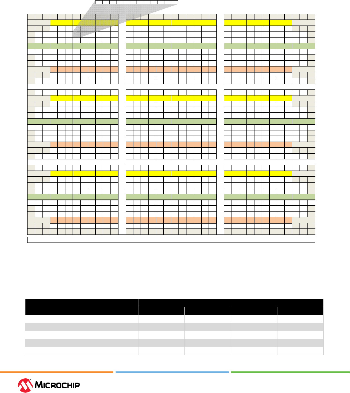
The fabric layout is shown in Figure 1. The FPGA logic resources are displayed as Logic Clusters (LC) and
Interface Logic (IL). Each LC and IL consists of 12 Logic Elements (LE). The embedded memory blocks and math
blocks are arranged in rows.
PolarFire Family Fabric User Guide
User Guide
© 2023 Microchip Technology Inc. and its subsidiaries
DS60001725G - 2
Figure 1. Fabric Layout
1 Logic Cluster = 12 Logic Elements
LE LE LE LE LE LE LE LE LE LE LE LE
M M M M M M M M M M
IL IL IL IL IL IL IL IL IL IL IL IL IL IL IL IL IL IL IL IL IL IL IL IL IL IL IL IL IL IL
LC LC LC LC LC LC LC LC LC LC LC LC LC LC LC LC LC LC LC LC LC LC LC LC LC LC LC LC LC LC LC LC LC LC
LC LC LC LC LC LC LC LC LC LC LC LC LC LC LC LC LC LC LC LC LC LC LC LC LC LC LC LC LC LC LC LC LC LC
R R R R R R R R R R R R
IL IL IL IL IL IL IL IL IL IL IL IL IL IL
IL IL IL IL IL IL IL IL IL IL IL IL IL IL IL IL IL IL IL IL IL IL
LC LC LC LC LC LC LC LC LC LC LC LC LC LC LC LC LC LC LC LC LC LC LC LC LC LC LC LC LC LC LC LC LC LC
LC LC LC LC LC LC LC LC LC LC LC LC LC LC LC LC LC LC LC LC LC LC LC LC LC LC LC LC LC LC LC LC LC LC
µ µ µ µ µ µ µ µ µ µ µ µ µ µ µ µ µ µ µ µ µ µ µ µ µ µ µ µ µ µ
IL IL IL IL IL IL IL IL IL IL IL IL IL IL
IL IL IL IL IL IL IL IL IL IL IL IL IL IL IL IL
LC LC LC LC LC LC LC LC LC LC LC LC LC LC LC LC LC LC LC LC LC LC LC LC LC LC LC LC LC LC LC LC LC LC
LC LC LC LC LC LC LC LC LC LC LC LC LC LC LC LC LC LC LC LC LC LC LC LC LC LC LC LC LC LC LC LC LC LC
M M M M M M M M M M
IL IL IL IL IL IL IL IL IL IL IL IL IL IL IL IL IL IL IL IL IL IL IL IL IL IL IL IL IL IL
LC LC LC LC LC LC LC LC LC LC
LC LC LC LC LC LC LC LC LC LC LC LC LC LC LC LC LC LC LC LC LC LC LC LC
LC LC LC LC LC LC LC LC LC LC LC LC LC LC LC LC LC LC LC LC LC LC LC LC LC LC LC LC LC LC LC LC LC LC
R R R R R R R R R R R R
IL IL IL IL IL IL IL IL IL IL IL IL IL IL IL IL IL IL IL IL IL IL IL IL IL IL IL IL IL IL IL IL IL IL IL IL
LC LC LC LC LC LC LC LC LC LC LC LC LC LC LC LC LC LC LC LC LC LC LC LC LC LC LC LC LC LC LC LC LC LC
LC LC LC LC LC LC LC LC LC LC LC LC LC LC LC LC LC LC LC LC LC LC LC LC LC LC LC LC LC LC LC LC LC LC
µ µ µ µ µ µ µ µ µ µ µ µ µ µ µ µ µ µ µ µ µ µ µ µ µ µ µ µ µ µ
IL IL IL IL IL IL IL IL IL IL IL IL IL IL IL IL IL IL IL IL IL IL IL IL IL IL IL IL IL IL
LC LC LC LC LC LC LC LC LC LC LC LC LC LC LC LC LC LC LC LC LC LC LC LC LC LC LC LC LC LC LC LC LC LC
LC LC LC LC LC LC LC LC LC LC LC LC LC LC LC LC LC LC LC LC LC LC LC LC LC LC LC LC LC LC LC LC LC LC
M M M M M M M M M M
IL IL IL IL IL IL IL IL IL IL IL IL IL IL IL IL IL IL IL IL IL IL IL IL IL IL IL IL IL IL
LC LC LC LC LC LC LC LC LC LC LC LC LC LC LC LC LC LC LC LC LC LC LC LC LC LC LC LC LC LC LC LC LC LC
LC LC LC LC LC LC LC LC LC LC LC LC LC LC LC LC LC LC LC LC LC LC LC LC LC LC LC LC LC LC LC LC LC LC
R R R R R R R R R R R R
IL IL IL IL IL IL IL IL IL IL IL IL IL IL IL IL IL IL IL IL IL IL IL IL IL IL IL IL IL IL IL IL IL IL IL IL
LC LC LC LC LC LC LC LC LC LC LC LC LC LC LC LC LC LC LC LC LC LC LC LC LC LC LC LC LC LC LC LC LC LC
LC LC LC LC LC LC LC LC LC LC LC LC LC LC LC LC LC LC LC LC LC LC LC LC LC LC LC LC LC LC LC LC LC LC
µ µ µ µ µ µ µ µ µ µ
µ µ µ µ µ µ µ µ µ µ µ µ µ µ µ µ µ µ µ µ
IL IL IL IL IL IL IL IL IL IL IL IL IL IL IL IL IL IL IL IL IL IL IL IL IL IL IL IL IL IL
LC – Logic cluster
IL – Interface logic
M – Math block
R – LSRAMs
µ – µSRAMs
µPROM
The following table lists the fabric resources available in the PolarFire devices.
Table 2. Fabric Resources in PolarFire Devices
Resources PolarFire
®
Devices
MPF100 MPF200 MPF300 MPF500
Logic elements (4LUT + DFF) 71,736 127,896 198,744 319,992
Interface logic 36,864 64,512 100,800 161,280
Total logic 108,600 192,408 299,544 481,272
LSRAM blocks (20 Kb each) 352 616 952 1,520
Total LSRAM bits (Mb) 6.87 12.03 18.59 29.69
User Guide
© 2023 Microchip Technology Inc. and its subsidiaries
DS60001725G - 3
...........continued
Resources PolarFire
®
Devices
MPF100 MPF200 MPF300 MPF500
μSRAM blocks (768 bits each) 1,008 1,764 2,772 4,440
Total μSRAM bits (Mb) 0.74 1.29 2.03 3.25
Total RAM (Mb) 7.6 13.32 20.62 32.94
Math blocks (18 × 18 MACC) 336 588 924 1,480
μPROM (Kb) 297 297 459 513
Note: 1 Kb = 1024 bits, 1 Mb = 1024 Kb.
The following table lists the fabric resources available in the PolarFire SoC devices.
Table 3. Fabric Resources in PolarFire SoC Devices
Resources PolarFire
®
SoC Devices
MPFS025 MPFS095 MPFS160 MPFS250 MPFS460
Logic elements (4LUT + DFF) 23,000 93,000 1,61,000 2,54,000 4,61,000
Interface logic 7,920 32,112 54,576 85,680 1,54,800
LSRAM blocks (20 Kb each) 84 308 520 812 1,460
μSRAM blocks (768 bits each) 204 876 1,494 2,352 4,260
Total RAM (Mb) 1.8 6.7 11.3 17.6 31.6
Math blocks (18 × 18 MACC) 68 292 498 784 1,420
μPROM (Kb) 194 387 415 470 553
Note: 1 Kb = 1024 bits, 1 Mb = 1024 Kb.
The following table lists the fabric resources available in the RT PolarFire devices.
Table 4. Fabric Resources in RT PolarFire Devices
Resources RT PolarFire
®
Devices
Logic elements (4LUT + DFF) 319,992
Interface logic 161,280
Total logic 481,272
LSRAM blocks (20 Kb each) 1,520
Total LSRAM bits (Mb) 29.69
μSRAM blocks (768 bits each) 4,440
Total μSRAM bits (Mb) 3.25
Total RAM (Mb) 32.94
Math blocks (18 × 18 MACC) 1,480
μPROM (Kb) 513
Note: 1 Kb = 1024 bits, 1 Mb = 1024 Kb.

User Guide
© 2023 Microchip Technology Inc. and its subsidiaries
DS60001725G - 4
Table of Contents
Introduction...........................................................................................................................................................................1
1. Logic Element and Routing.......................................................................................................................................... 5
1.1. Logic Element..................................................................................................................................................... 5
1.2. Interface Logic.................................................................................................................................................... 5
1.3. Logic Cluster....................................................................................................................................................... 8
1.4. Routing Architecture..........................................................................................................................................8
1.5. Fabric X-Y Coordinates...................................................................................................................................... 8
2. Embedded Memory Blocks........................................................................................................................................ 10
2.1. LSRAM............................................................................................................................................................... 11
2.2. μSRAM............................................................................................................................................................... 36
2.3. μPROM.............................................................................................................................................................. 45
2.4. sNVM................................................................................................................................................................. 59
2.5. eNVM (PolarFire SoC Only)............................................................................................................................. 60
3. Math Blocks..................................................................................................................................................................61
3.1. Features............................................................................................................................................................ 61
3.2. Math Block Resources..................................................................................................................................... 61
3.3. Functional Description.................................................................................................................................... 61
3.4. Cascading Math Blocks....................................................................................................................................66
3.5. Operational Modes..........................................................................................................................................68
3.6. Implementation............................................................................................................................................... 71
4. Appendix: Supported Memory File Formats for LSRAM and μSRAM....................................................................79
4.1. Write Port Width Alignment............................................................................................................................81
5. Appendix: Macro Conguration................................................................................................................................ 88
5.1. LSRAM Macro................................................................................................................................................... 88
5.2. μSRAM Macro................................................................................................................................................... 95
5.3. Math Block Macro............................................................................................................................................ 97
5.4. Libero SoC Compile Report.......................................................................................................................... 109
6. References................................................................................................................................................................. 113
7. Revision History.........................................................................................................................................................114
Microchip FPGA Support..................................................................................................................................................117
Microchip Information..................................................................................................................................................... 117
The Microchip Website............................................................................................................................................. 117
Product Change Notication Service...................................................................................................................... 117
Customer Support.................................................................................................................................................... 117
Microchip Devices Code Protection Feature..........................................................................................................117
Legal Notice............................................................................................................................................................... 118
Trademarks................................................................................................................................................................ 118
Quality Management System.................................................................................................................................. 119
Worldwide Sales and Service...................................................................................................................................120
Logic Element and Roung
User Guide
© 2023 Microchip Technology Inc. and its subsidiaries
DS60001725G - 5
1. Logic Element and Roung (Ask a Queson)
The fabric includes an array of logic elements grouped in clusters connected by hierarchical
routing structures. These clusters are arranged in rows and are used to implement sequential and
combinational logic. See Figure 1-7 and Figure 1-8 for PolarFire and PolarFire SoC fabric coordinates
respectively.
1.1 Logic Element (Ask a Queson)
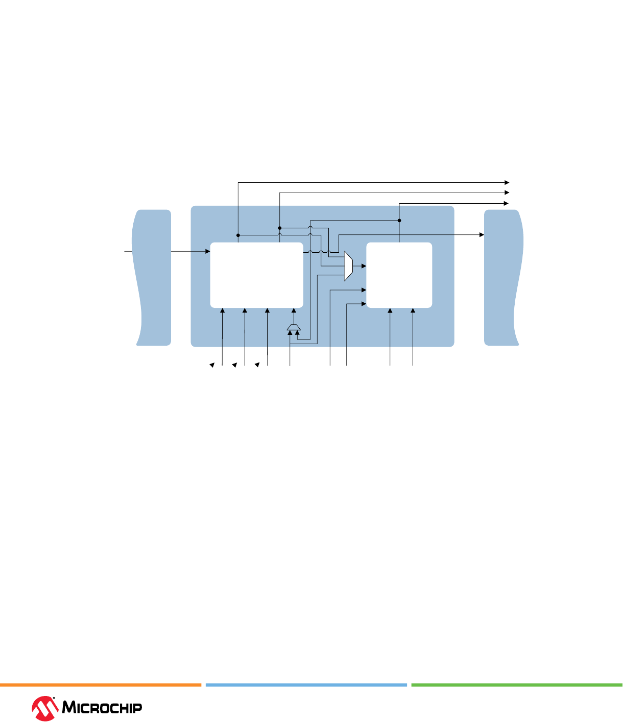
The logic element consists of a 4-input Lookup Table (LUT) with a carry chain and D-type ip-
op, as shown in Figure 1-1. The logic element is fracturable, which means that the LUT can be
independently used without ip-op, or ip-op can be used without LUT.
Figure 1-1. Funconal Block Diagram of Logic Element
Logic Element
SUM (S)
Y
4-LUT
with Carry Chain
D1
data
Cout
Cout
Cin
Q
EN CLK SLn ALn
Cin
S
Y
Cout
D
A B C
C
BA
Logic Element
Cin
Logic Element
ALn
Flip-Flop
D
EN
CLK
SLn
Q
The 4-input LUT with carry chain can be
congured to implement any 4-input combinational logical
function or arithmetic function. The 4-input LUT generates the output (Y) depending on the four
inputs—A, B, C, and D. The carry chain is implemented using a 3-bit carry-look-ahead circuit. This
circuit is connected between various logic elements by carry chain input (Cin) signal and carry chain
output (Cout) signal. When the LUT is used to implement arithmetic functions, the carry chain input
(Cin) is used with LUT output to generate the Sum (S) output. However, for non-arithmetic functions,
the sum (S) output can still be used as an output along with the other output (Y).
The D-type ip-op can be used as a register or latch. The data input (D) of the D-type ip-op
can be sourced from one of three inputs: the direct input (D1), the combinational output (Y) of the
LUT, or the sum output (S) of the LUT (Figure 1-1). The ALn and SLn are asynchronous load and
synchronous load active-low signals that can be congured as reset signal. The ip-op output (Q)
can be an output of the logic element or one of the data inputs to the 4-input LUT (inside the same
logic element).
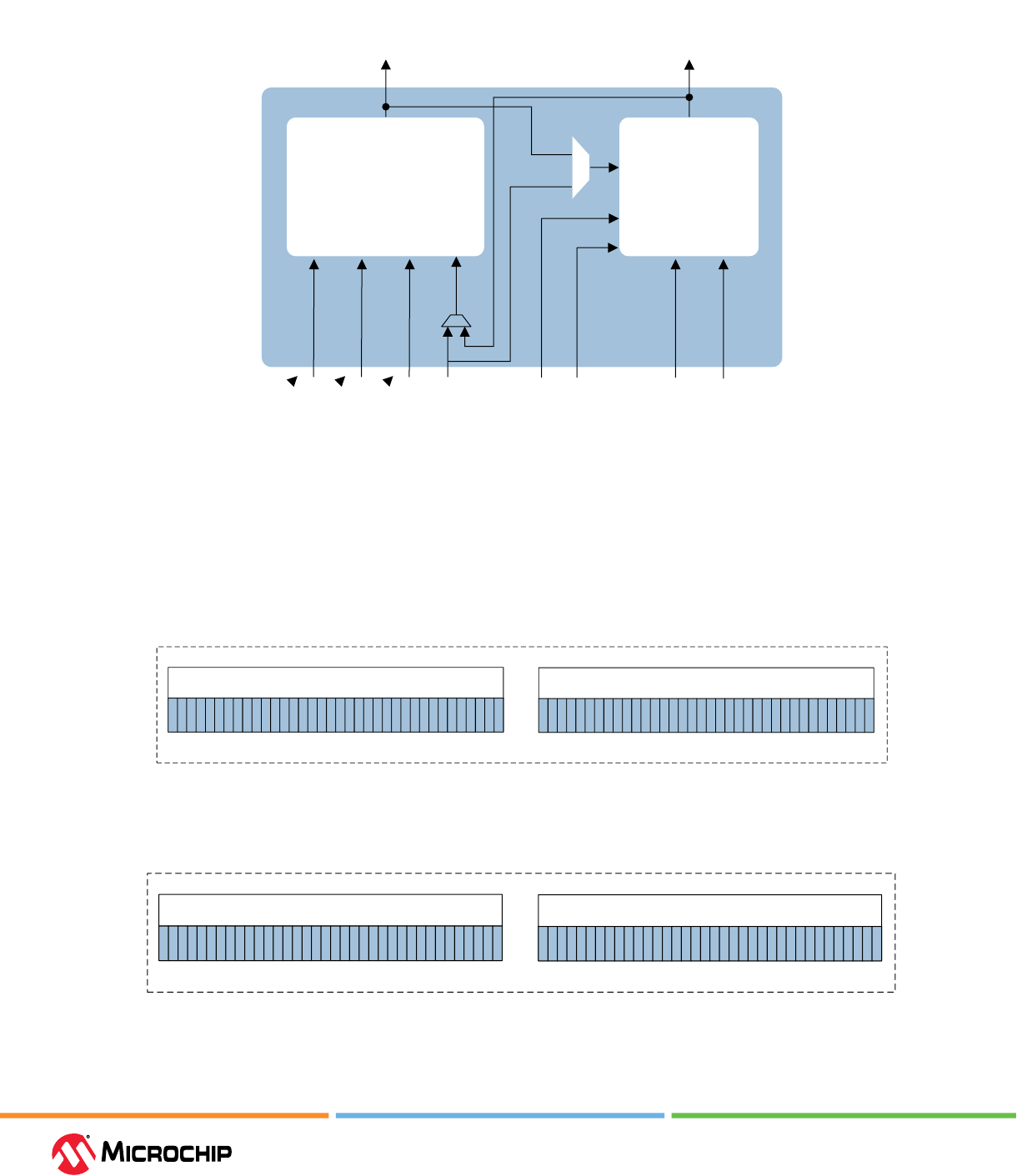
1.2 Interface Logic (Ask a Queson)
The embedded hard IP blocks (LSRAM, μSRAM, and Math blocks) are connected to the fabric through
Interface Logic (ILs).
The following table lists the total number of ILs associated with each memory block in the PolarFire
devices.
Logic Element and Roung
User Guide
© 2023 Microchip Technology Inc. and its subsidiaries
DS60001725G - 6
Table 1-1. ILs for Embedded Hard IP Blocks (PolarFire Devices)
Resources MPF100 MPF200 MPF300 MPF500
No. of
Blocks
No. of ILs No. of
Blocks
No. of ILs No. of
Blocks
No. of ILs No. of
Blocks
No. of ILs
LSRAM 352 12,672 616 22,176 952 34,272 1,520 54,720
μSRAM 1008 12,096 1,764 21,168 2,772 33,264 4,440 53,280
Math block 336 12,096 588 21,168 924 33,264 1,480 53,280
Total interface logic — 36,864 — 64,512 — 100,800 — 161,280
The following table lists the total number of ILs associated with each memory block in the PolarFire
SoC devices.
Table 1-2. ILs for Embedded Hard IP Blocks (PolarFire SoC Devices)
Resources MPFS025 MPFS095 MPFS160 MPFS250 MPFS460
No. of
Blocks
No. of
ILs
No. of
Blocks
No. of
ILs
No. of
Blocks
No. of
ILs
No. of
Blocks
No. of
ILs
No. of
Blocks
No. of
ILs
LSRAM 84 3024 308 11088 520 18720 812 29232 1460 52560
μSRAM 204 2448 876 10512 1494 17928 2352 28224 4260 51120
Math block 68 2448 292 10512 498 17928 784 28224 1420 51120
Total interface
logic
— 7920 — 32112 — 54576 — 85680 — 154800
The following table lists the total number of ILs associated with each memory block in the RT
PolarFire devices.
Table 1-3. ILs for Embedded Hard IP Blocks (RT PolarFire Devices)
Resources RT PolarFire
®
Devices
No. of Blocks No. of ILs
LSRAM 1,520 54,720
μSRAM 4,440 53,280
Math block 1,480 53,280
Total interface logic — 161,280
The ILs are structurally similar to LEs with a 4-input LUT and D-type ip-op, but without a dedicated
carry chain, as shown in the following gure.
Logic Element and Roung
User Guide
© 2023 Microchip Technology Inc. and its subsidiaries
DS60001725G - 7
Figure 1-2. Funconal Block Diagram of Interface Logic
Flip-Flop4-LUT
Interface Logic
D1
ALn
data
D
EN
CLK
SLn
Q
CBA EN CLK SLn ALn
A B C
D
Y
Each LSRAM and Math block is associated with 36 ILs, and each μSRAM is associated with 12 ILs. For
more information, see Figure 1-3, Figure 1-4, and Figure 1-5.
If an embedded hard IP block is used in a design, the associated ILs connect the ports of the
embedded hard IP blocks to the fabric routing. Any IL that is not utilized by an embedded hard IP
block is automatically available for user logic.
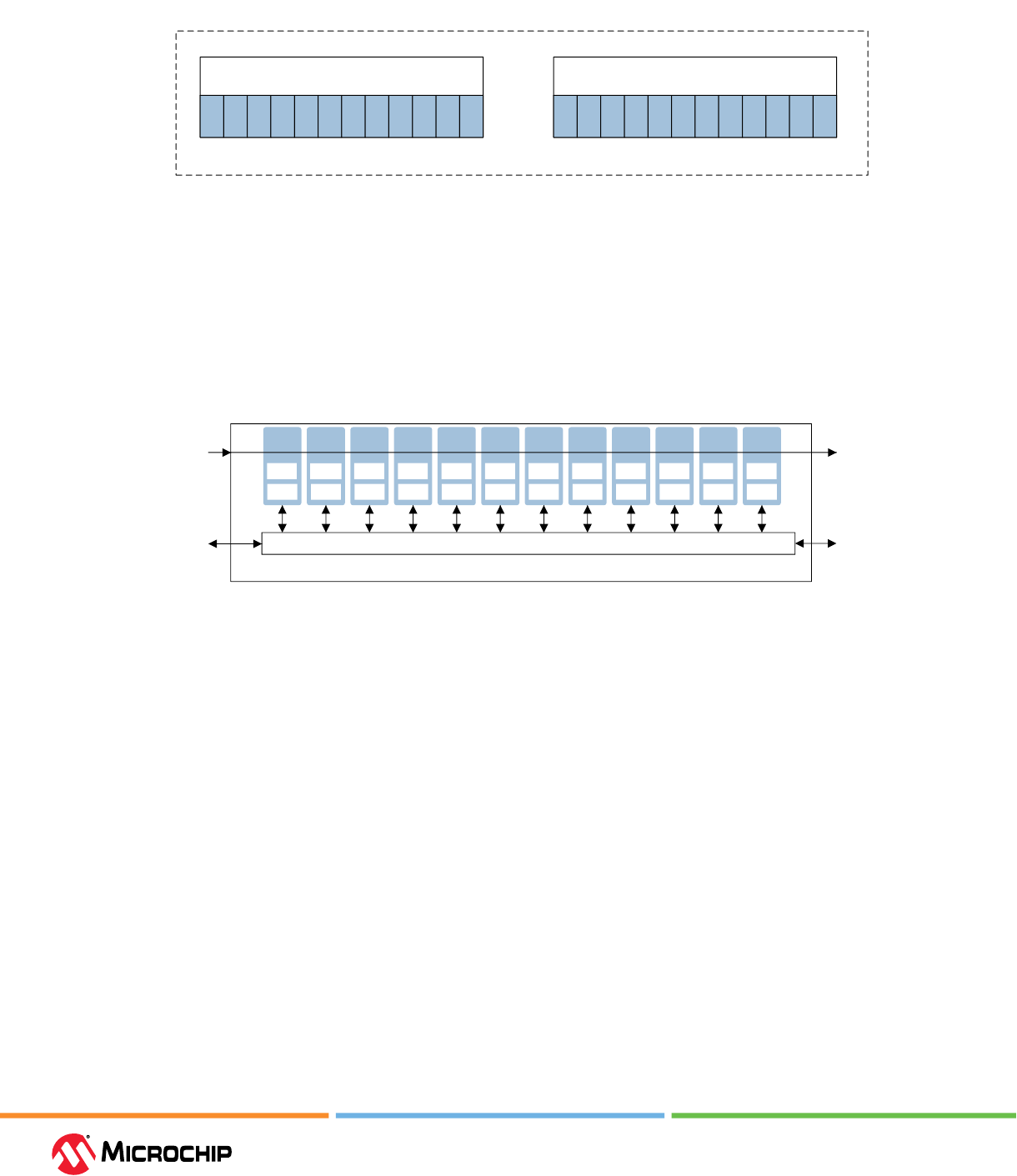
Figure 1-3. LSRAM Interfacing with ILs in a Row
Row
...
36 Interface Logic 36 Interface Logic
LSRAM
LSRAM
I
L
I
L
I
L
I
L
I
L
I
L
I
L
I
L
I
L
I
L
I
L
I
L
I
L
I
L
I
L
I
L
I
L
I
L
I
L
I
L
I
L
I
L
I
L
I
L
I
L
I
L
I
L
I
L
I
L
I
L
I
L
I
L
I
L
I
L
I
L
I
L
I
L
I
L
I
L
I
L
I
L
I
L
I
L
I
L
I
L
I
L
I
L
I
L
I
L
I
L
I
L
I
L
I
L
I
L
I
L
I
L
I
L
I
L
I
L
I
L
I
L
I
L
I
L
I
L
I
L
I
L
I
L
I
L
I
L
I
L
I
L
I
L
Figure 1-4. Math Block Interfacing with ILs in a Row
Row
...
36 Interface Logic 36 Interface Logic
Math Block
Math Block
I
L
I
L
I
L
I
L
I
L
I
L
I
L
I
L
I
L
I
L
I
L
I
L
I
L
I
L
I
L
I
L
I
L
I
L
I
L
I
L
I
L
I
L
I
L
I
L
I
L
I
L
I
L
I
L
I
L
I
L
I
L
I
L
I
L
I
L
I
L
I
L
I
L
I
L
I
L
I
L
I
L
I
L
I
L
I
L
I
L
I
L
I
L
I
L
I
L
I
L
I
L
I
L
I
L
I
L
I
L
I
L
I
L
I
L
I
L
I
L
I
L
I
L
I
L
I
L
I
L
I
L
I
L
I
L
I
L
I
L
I
L
I
L
Logic Element and Roung
User Guide
© 2023 Microchip Technology Inc. and its subsidiaries
DS60001725G - 8
Figure 1-5. μSRAMs Interfacing with ILs in a Row
Row
...
12 Interface Logic 12 Interface Logic
µSRAM µSRAM
I
L
I
L
I
L
I
L
I
L
I
L
I
L
I
L
I
L
I
L
I
L
I
L
I
L
I
L
I
L
I
L
I
L
I
L
I
L
I
L
I
L
I
L
I
L
I
L
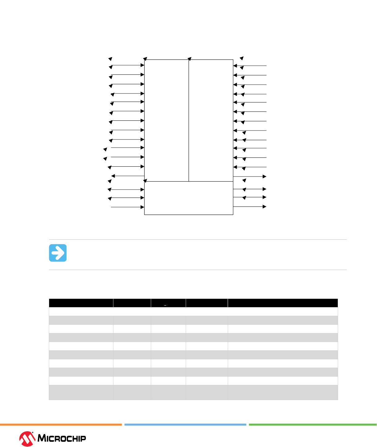
1.3 Logic Cluster (Ask a Queson)
The logic elements in the FPGA fabric are organized in clusters. A logic cluster is a group of 12 LEs.
Each logic cluster is connected by a routing interface that connects to its associated LEs and the
adjacent routing interfaces.
The following gure shows the logic cluster with its routing interface.
Figure 1-6. Logic Cluster
Routing Interface
Adjacent
Routing
Interface
Adjacent
Routing
Interface
FF FF FF FF FF FF FF FF FF FF FF FF
LE
LE
LE
LE
LE
LE
LE
LE
LE
LE
LE
LE
Carry In
Carry Out
Logic Cluster
LUT
LUT
LUT
LUT
LUT
LUT
LUT
LUT
LUT
LUT
LUT
LUT
1.4 Roung Architecture (Ask a Queson)
The PolarFire family supports two types of routings—intra-cluster routing and inter-cluster routing.
The intra-cluster routing connects the LEs within a cluster, and inter-cluster routing connects LEs
between multiple clusters. The intra-cluster routing has lower propagation delay compared to inter-
cluster routing. When connecting the adjacent clusters, inter-cluster routing also has additional
short routing connections for faster routing.
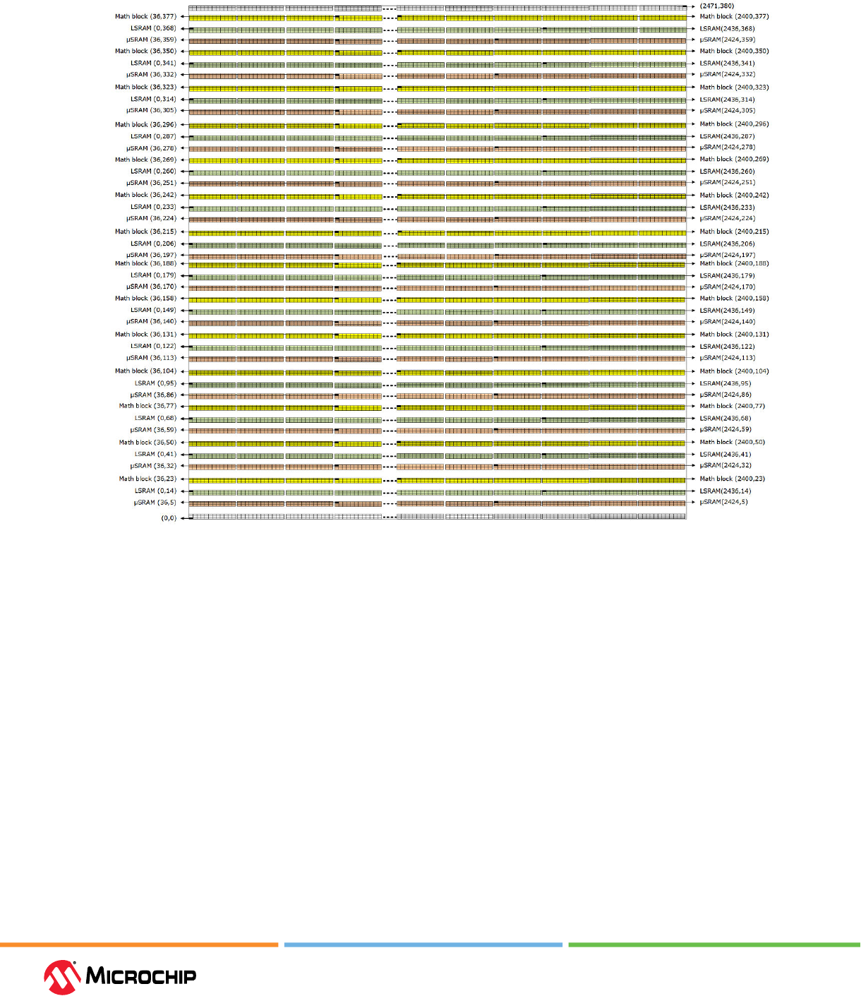
1.5 Fabric X-Y Coordinates (Ask a Queson)
Each 4-input LUT, D-type ip-op, carry chain, LSRAM, μSRAM, and Math block has individual X-Y
coordinates. For manual placement of these blocks, it is possible to set region constraints using
these coordinates. The coordinates are measured from the lower left (0, 0) to the top right corner (X,
Y); where X, Y values vary for each device. For more details, see SmartTime User Guide, I/O Editor User
Guide, and ChipPlanner User Guide on Libero SoC Design Resources page.
The following gure shows the available X-Y coordinates of LSRAM, μSRAM, and Math block for
placement constraints for the PolarFire MPF300 device.
Logic Element and Roung
User Guide
© 2023 Microchip Technology Inc. and its subsidiaries
DS60001725G - 9
Figure 1-7. MPF300 Fabric X-Y Coordinates
Figure 1-8 shows the available X-Y coordinates of LSRAM, μSRAM, and Math block for placement
constraints for the PolarFire SoC MPFS250 device.
Figure 1-8. MPFS250 Fabric X-Y Coordinates
To be updated.
The following gure shows the available X-Y coordinates of LSRAM, μSRAM, and Math block for
placement constraints for the RT PolarFire RTPF500 device.
Figure 1-9. RTPF500 Fabric X-Y Coordinates
To be updated.

Embedded Memory Blocks
User Guide
© 2023 Microchip Technology Inc. and its subsidiaries
DS60001725G - 10
2. Embedded Memory Blocks (Ask a Queson)
The PolarFire family has the following memory blocks:
• LSRAM—The embedded large SRAM blocks are 20Kbits each with 20-bit width and a depth of
1024 locations. The LSRAMs can be congured as either dual port or two port memories. The
number of LSRAMs available in a device varies as shown in Table 2 and Table 3. The LSRAMs
support ECC when congured in 33-bit data width in two-port mode. LSRAMs can be congured
in various modes as shown in Table 2-1. LSRAMs can be initialized with user data during power-
up.
• μSRAM—The embedded 768-bit SRAM blocks (RAM64x12) are arranged in multiple rows within
the fabric and can be accessed through the fabric routing architecture. The number of available
μSRAM blocks depends on the specic device, as shown in Table 2 and Table 3. μSRAMs can be
initialized during power-up.
• μPROM—The embedded non-volatile PROM is arranged in a single row at the bottom of the
fabric and is read only through the fabric interface. μPROM is programmed with the FPGA
bitstream during fabric programming and it cannot be programmed independently. μPROM is
used to store the initialization data for LSRAM and μSRAM and other user data.
• sNVM—Each PolarFire FPGA has 56 KB of Secure Non-volatile Memory (sNVM). The sNVM can
be used to initialize LSRAM and μSRAMs with secure data. sNVM can be accessed through the
system services.
Along with the above memory blocks, the PolarFire SoC family includes the following memory block:
• eNVM (PolarFire SoC Only)—The 128 KB of eNVM is located in the MSS. eNVM is used to store the
rst stage bootloader program for booting the E51 monitor core. eNVM is programmed with the
device bitstream during the device programming, it cannot be programmed independently.
The following table lists the features of the memory blocks of the PolarFire family.
Table 2-1. LSRAM, μSRAM, μPROM, and sNVM Features
Feature LSRAM
(PolarFire, PolarFire
SoC, and RT PolarFire)
μSRAM (PolarFire,
PolarFire SoC, and
RT PolarFire)
μPROM
(PolarFire,
PolarFire SoC,
and RT PolarFire)
sNVM (PolarFire,
PolarFire SoC,
and RT PolarFire)
eNVM (Only
PolarFire SoC)
Memory size 20,480 bits/block 768-bit/block See Table 2 and
Table 3
56 Kbytes 128 Kbytes
Memory
Conguration
Options
16K × 1, 8K × 2, 4K × 5,
2K × 10, 1K × 20, 512
× 40
1
, and 512 × 33
1
(with ECC)
64 × 12 Up to 64K × 9 Not Applicable Not Applicable
Number of ports 2 read ports, 2 write
ports
1 read port, 1 write
port
1 read port Not Applicable Not Applicable
Memory modes True dual-port and
two-port
Two-port Single-port Not Applicable Not Applicable
Read operation Synchronous Synchronous/
Asynchronous
Asynchronous Through system
service calls
Asynchronous
Write operation Simple write, feed-
through write, and
read-before-write
Simple write Only during
device
programming
During device
programming
and System
Service calls
During device
programming
ECC Available for two-port
mode (512 × 33) only
Not available Not Applicable Not Applicable Not Applicable
Note:
1. ×40 and ×33 are only available in two-port mode.
Embedded Memory Blocks
User Guide
© 2023 Microchip Technology Inc. and its subsidiaries
DS60001725G - 11
2.1 LSRAM (Ask a Queson)
Each LSRAM has two independent ports—Port A and Port B, as shown in Figure 2-1. Both these ports
support write and read operations, and can be congured in dual-port mode or two-port mode.
Figure 2-1. LSRAM Input/Output
Port A Port B
Common Signals
A_ADDR[13:0]
A_BLK_EN[2:0]
A_CLK
A_DIN[19:0]
A_DOUT[19:0]
B_ADDR[13:0]
B_BLK_EN[2:0]
B_CLK
B_DIN[19:0]
B_DOUT[19:0]
A_WEN[1:0]
A_REN
A_WIDTH[2:0]
A_WMODE[1:0]
A_BYPASS
A_DOUT_EN
A_DOUT_SRST_N
A_DOUT_ARST_N
ECC_EN
ECC_BYPASS
BUSY_FB
B_WEN[1:0]
B_REN
B_WIDTH[2:0]
B_WMODE[1:0]
B_BYPASS
B_DOUT_EN
B_DOUT_SRST_N
B_DOUT_ARST_N
SB_CORRECT
DB_DETECT
ACCESS_BUSY
Important: When ECC is enabled, if a single-bit error occurs in a word, the data is
corrected. If multiple-bit errors occur in a word, the data from the LSRAM is not corrected
or modied.
The following table lists the ports of LSRAM.
Table 2-2. LSRAM Port List
Port Name Direction Type
1
Polarity Description
Port A
A_ADDR[13:0] Input Dynamic — Port A address
A_BLK_EN[2:0] Input Dynamic Active high Port A block selects
A_CLK Input Dynamic Rising edge Port A clock
A_DIN[19:0] Input Dynamic — Port A write-data
A_DOUT[19:0] Output Dynamic — Port A read-data
A_WEN[1:0] Input Dynamic Active high Port A byte write-enables
A_REN Input Dynamic Active high Port A read-enable
A_WIDTH[2:0] Input Static — Port A width/depth mode select
A_WMODE[1:0] Input Static Active high Port A read-before-write and feed-through
write selects
Embedded Memory Blocks
User Guide
© 2023 Microchip Technology Inc. and its subsidiaries
DS60001725G - 12
...........continued
Port Name Direction Type
1
Polarity Description
A_BYPASS Input Static Active high Port A read data pipeline register bypassed
when High
A_DOUT_EN Input Dynamic Active high Port A pipeline register enable
A_DOUT_SRST_N Input Dynamic Active low Port A pipeline register synchronous-reset
A_DOUT_ARST_N Input Dynamic Active low Port A pipeline register asynchronous-reset
Port B
B_ADDR[13:0] Input Dynamic — Port B address
B_BLK_EN[2:0] Input Dynamic Active high Port B block selects
B_CLK Input Dynamic Rising edge Port B clock
B_DIN[19:0] Input Dynamic — Port B write-data
B_DOUT[19:0] Output Dynamic — Port B read-data
B_WEN[1:0] Input Dynamic Active high Port B write-enables (per byte)
B_REN Input Dynamic Active high Port B read-enable
B_WIDTH[2:0] Input Static Mode select Port B width/depth
B_WMODE[1:0] Input Static Active high Port B read-before-write and feed-through
write selects
B_BYPASS Input Static Active high Port B read data pipeline register bypassed
when High
B_DOUT_EN Input Dynamic Active high Port B pipeline register enable
B_DOUT_SRST_N Input Dynamic Active low Port B pipeline register synchronous-reset
B_DOUT_ARST_N Input Dynamic Active low Port B pipeline register asynchronous-reset
Common Signals
ECC_EN Input Static Active high Enable ECC
ECC_BYPASS Input Static Active high ECC pipeline register bypassed when High.
SB_CORRECT Output Dynamic Active high Single-bit correct ag
DB_DETECT Output Dynamic Active high Dual-bit error detect ag
BUSY_FB Input Static Active high Lock access to SmartDebug
ACCESS_BUSY Output Dynamic Active high Busy signal from SmartDebug
Note:
1. Static inputs are tied to 0 or 1 during design implementation.
2.1.1 Dual-Port Mode (Ask a Queson)
The LSRAM block can be congured as a true dual-port SRAM with independent write and read
ports, as shown in Figure 2-2. Write and read operations can be performed from both ports (A
and B) independently at any location as long as there is no write collision. Each port has a unique
address, data in, data out, clock, block select, write enable, pipeline registers, and feed-through
MUXes.
Embedded Memory Blocks
User Guide
© 2023 Microchip Technology Inc. and its subsidiaries
DS60001725G - 13
Figure 2-2. Simplied Funconal Block Diagram of LSRAM in Dual-Port Mode
A_DOUT[19:0]
A_DIN[19:0]
B_DIN[19:0]
A_ADDR[13:0]
A_WEN[1:0]
A_BLK_EN[2:0]
A_CLK
Port A Row Decode
Write Control
Port B Row Decode
Write Control
Column
Decode
Column
Decode
B_DOUT[19:0]
Memory Array
B_REN
B_DOUT_EN
A_REN
B_DOUT_ARST_N
B_DOUT_SRST_N
A_DOUT_EN
A_DOUT_SRST_N
A_DOUT_ARST_N
B_CLK
A_CLK
20
20
20
20
Pipeline
Register A
Pipeline
Register B
A_WIDTH[2:0]
A_WMODE[1:0]
B_ADDR[13:0]
B_WEN[1:0]
B_BLK_EN[2:0]
B_CLK
B_WIDTH[2:0]
B_WMODE[1:0]
A_BYPASS
B_BYPASS
2.1.1.1 Dual-Port Data Width Conguraon (Ask a Queson)
In Dual-Port mode, both ports A and B have maximum data width of x20. Each port can be
congured in multiple data widths. The conguration of one port has a corresponding conguration
for the other port, as shown in Table 2-3.
Table 2-3. Port A and Port B Data Width Conguraons for LSRAM
Port A Data Width Port B Data Width
x1 x1, x2, x4, x8, x16
x2 x1, x2, x4, x8, x16
x4 x1, x2, x4, x8, x16
x5 x5, x10, x20
x8 x1, x2, x4, x8, x16
x10 x5, x10, x20
x16 x1, x2, x4, x8, x16
x20 x5, x10, x20
2.1.1.2 Block Select Operaon (Ask a Queson)
In Dual-Port mode, to perform two independent write and read operations (on Port A, Port B, or
both) the block select signal is required. Table 2-4 lists the block select operation for Port A and Port
B.
Table 2-4. Block Select Operaon
A_BLK_EN[2:0] B_BLK_EN[2:0] Operation
Any one bit = 0 Any one bit = 0 No operation on Port A or B. The data output A_DOUT[19:0] and
B_DOUT[19:0] will be forced zero.
Embedded Memory Blocks
User Guide
© 2023 Microchip Technology Inc. and its subsidiaries
DS60001725G - 14
...........continued
A_BLK_EN[2:0] B_BLK_EN[2:0] Operation
Any one bit = 0 111 Read or write operation on Port B
111 Any one bit = 0 Read or write operation on Port A
111 111 Read or write operation on both Ports A and B
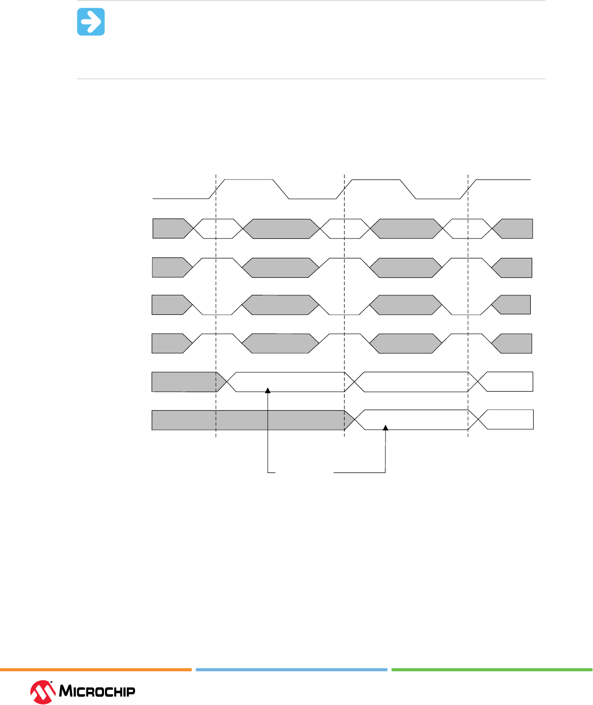
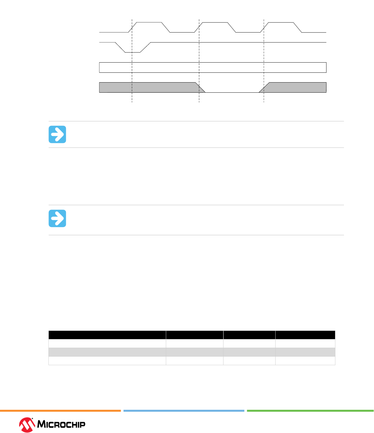
When the pipeline registers are enabled, the eect of the block select at the outputs is delayed by
one clock cycle, as shown in the following gure.
Figure 2-3. Block Select Inputs for Dual-Port Mode
A_CLK
B_CLK
A_BLK_EN
B_BLK_EN
Non-Pipeline Mode
B_DOUT[19:0]
A_DOUT[19:0]
B_DOUT[19:0]
A_DOUT[19:0]
Pipeline Mode
Clock Cycle #1 Clock Cycle #2 Clock Cycle #3
20'b0
20'b0
2.1.1.3 Byte Write Enables (Ask a Queson)
The byte write enables (A_WEN[1:0], B_WEN[1:0]) enable writing individual bytes of data for x20 and
x16 widths. The byte write enables for Port A (A_WEN[1:0]) enables A_DIN[19:10] and A_DIN[9:0]
respectively. The byte write enables for Port B (B_WEN[1:0]) enable B_DIN[19:10] and B_DIN[9:0]
respectively.
The byte write enables are also used in x1, x2, x4, x5, x8, x10, x16, and x20 widths to select the
operational mode (read/write) for a Port A or Port B. If all byte write enables are low, then Port A or
Port B is considered to be in read mode and any read operations are controlled by the read enables
(A_REN/B_REN).
Table 2-5 lists the byte write enable settings for Port A and Port B.
Table 2-5. Byte Write Enables Sengs for Dual-Port Mode
Depth x Width A_WEN/B_WEN Result
16K x 1, 8K x 2, 4K x 4, 4K x 5, 2K x 8, 2K x 10 00 or 10 Perform a read operation
01 or 11 Perform a write operation
1K x 16 00 Perform a read operation
01 Write [7:0]
10 Write [17:10]
11 Write [17:10], [7:0]
1K x 20 00 Perform a read operation
01 Write [9:0]
10 Write [19:10]
11 Write [19:0]
2.1.1.4 Read Enable (Ask a Queson)
The read enable signals, A_REN and B_REN, perform the read operation on ports A and B. When
read enable is low, the data outputs retain their previous state and no dynamic read power is
Embedded Memory Blocks
User Guide
© 2023 Microchip Technology Inc. and its subsidiaries
DS60001725G - 15
consumed on that port. When read enable is high, LSRAM performs read operations and consumes
read power.
2.1.1.5 Synchronous Pipeline Register Reset (Ask a Queson)
Each pipeline register has one synchronous reset. In dual-port mode, A_DOUT_SRST_N and
B_DOUT_SRST_N drive the synchronous reset of the data output pipeline registers—A_DOUT and
B_DOUT. If the synchronous pipeline reset is low, the pipeline data output registers are reset to zero
on the next valid clock edge, as shown in the following gure.
Figure 2-4. Synchronous Pipeline Register Reset in Dual-Port Mode
A_CLK
B_CLK
A_DOUT_SRST_N
B_DOUT_SRST_N
A_DOUT[19:0]
B_DOUT[19:0]
A_DOUT[19:0]
B_DOUT[19:0]
Non-Pipeline Mode
Pipeline Mode
Clock Cycle #1 Clock Cycle #2
No Change
20'b0
2.1.1.6 Asynchronous Pipeline Register Reset (Ask a Queson)
Each pipeline register has one asynchronous reset. In dual-port mode, A_DOUT_ARST_N and
B_DOUT_ARST_N drive the asynchronous reset of the data output pipeline registers—A_DOUT and
B_DOUT. If the asynchronous pipeline reset is driven low, the pipeline data output registers are
immediately reset to zero, as shown in the following gure.
Figure 2-5. Asynchronous Pipeline Register Reset in Dual-Port Mode
A_CLK
B_CLK
A_DOUT[19:0]
B_DOUT[19:0]
A_DOUT[19:0]
B_DOUT[19:0]
Non-Pipeline Mode
Pipeline Mode
A_DOUT_ARST_N
B_DOUT_ARST_N
Clock Cycle #1 Clock Cycle #2
No Change
20'b0
2.1.1.7 Read Operaon (Ask a Queson)
In dual-port mode, LSRAM supports both pipelined and non-pipelined read operations. In a
pipelined read operation, the output data is registered at the pipeline registers; as a result the
data is available on the corresponding data output on the next clock cycle.
In a non-pipelined read operation, the pipeline registers are bypassed and read data is available on
the output port in the same clock cycle.
Embedded Memory Blocks
User Guide
© 2023 Microchip Technology Inc. and its subsidiaries
DS60001725G - 16
Important:
• For high-performance designs, It is recommended to use the LSRAM with pipeline mode
to meet the design timing constraints.
• When multiple depth-cascaded blocks are used, A_REN and B_REN ports of Dual-Port
SRAM are disabled by the congurator GUI.
The following gure shows the timing for both pipelined and non-pipelined read operations in the
Dual-Port mode.
Figure 2-6. Read Operaon in Dual-Port Mode
A_REN
B_REN
A_CLK
B_CLK
A_WEN[1:0]
B_WEN[1:0]
A_ADDR[13:0]
B_ADDR[13:0]
A_DOUT_EN
B_DOUT_EN
A_DOUT[19:0]
B_DOUT[19:0]
A_DOUT[19:0]
B_DOUT[19:0]
Pipeline Mode
Non-Pipeline Mode
Clock Cycle #1 Clock Cycle #2
Data in address A0
D(A0)
D(A1)
D(A2)
D(A0)
D(A1)
A0
A1
A2
2.1.1.8 Write Operaon (Ask a Queson)
In dual-port mode, LSRAM supports the following write operations:
• 2.1.1.8.1. Simple Write
• 2.1.1.8.2. Feed-Through Write
• 2.1.1.8.3. Read-Before-Write
The type of write operation is specied while creating or conguring LSRAM in Libero SoC. For more
information on LSRAM conguration, see 2.1.3.2. LSRAM Congurator

Embedded Memory Blocks
User Guide
© 2023 Microchip Technology Inc. and its subsidiaries
DS60001725G - 17
Note: In dual-port mode, simultaneous write operations from both ports to the same address
location are not prevented. As simultaneous write operations can result in data uncertainty, it is
recommended to use external logic in the fabric to avoid collisions.
2.1.1.8.1 Simple Write (Ask a Queson)
In a simple-write operation, data input A_DIN and B_DIN are written to the corresponding address
locations A_ADDR and B_ADDR. The data written to the memory is available at the output only after
performing a read operation.
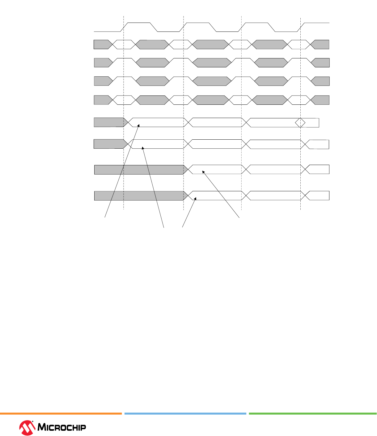
2.1.1.8.2 Feed-Through Write (Ask a Queson)
In a feed-through write operation for pipelined operations, the read data is available on the data
output bus on the next clock cycle. For non-pipelined operations, data written to the memory is
available in the same clock cycle on the corresponding data output bus. For more information, see
Figure 2-7.
In dual-port mode during feed-through write, the data output of each port can change in one of the
following ways:
• During read port reset, the data output becomes zero.
• If the block select input (A_BLK_EN) of Port A or B is driven low, then the corresponding port's
data output becomes zero.
• During valid write operations when read enable (A_REN and B_REN) is high, then write data is
available at the data output.
• If there is a valid read operation, then the read data is available at the data output. A valid
read happens when read enable (A_REN and B_REN) inputs are high, and byte write enable
(A_WEN[1:0] and B_WEN[1:0]) inputs are zero.
2.1.1.8.3 Read-Before-Write (Ask a Queson)
In a read-before-write operation for pipeline mode, read data is available on the data output bus
on the next clock cycle. For non-pipeline mode, the previous memory data from the current write
address is available on the data output before the new data is written to the address location. For
more information, see Figure 2-7.
In Dual-Port mode during read-before-write operations, the data output of each port can change in
one of the following ways:
• During read port reset, the data output becomes zero.
• If the block select input (A_BLK_EN) of Port A or B is driven low, then the corresponding port's
data output becomes zero.
• During valid write operations when read enables (A_REN and B_REN) are driven high, the previous
memory data from the current address is available on the data output before the new data is
written to the address location.
• If there is a valid read operation, then the read data is available on the data output. A valid read
happens when read enable (A_REN and B_REN) inputs are driven high, and byte write enable
(A_WEN[1:0] and B_WEN[1:0]) inputs are driven low.
The following gure shows the timing for feed-through-write and read-before-write operations for
Dual-Port mode.
Embedded Memory Blocks
User Guide
© 2023 Microchip Technology Inc. and its subsidiaries
DS60001725G - 18
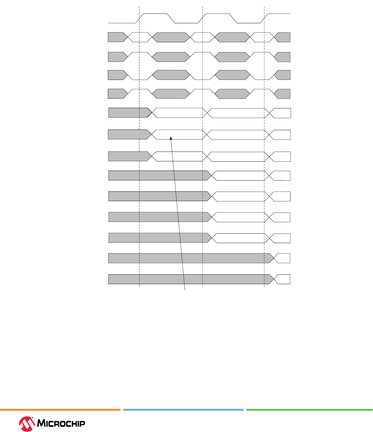
Figure 2-7. Write Operaons in Dual-Port Mode
A_CLK
B_CLK
A_ADDR[]
B_ADDR[]
A_DOUT_EN
B_DOUT_EN
A_WEN[1:0]
B_WEN[1:0]
A_DIN[]
B_DIN[]
A_DOUT[]
B_DOUT[]
A_DOUT[]
B_DOUT[]
Feed-Through Write Pipeline Mode
Feed-Through Write Non-Pipeline Mode
D0
Clock Cycle #1 Clock Cycle #2 Clock Cycle #3
D3
D0
D1 D2 D3
D0
D1
D2
A_DOUT[]
B_DOUT[]
A_DOUT[]
B_DOUT[]
Read Before Write Pipeline Mode
Read Before Write Non-Pipeline Mode
Previous data in Address A0
Current write data in Address A0
Current write data in Address A0
D1
A0
A1 A2 A3
D2
D(A0)
D(A3)
D(A1)
D(A2)
D(A0)
D(A1)
D(A2)
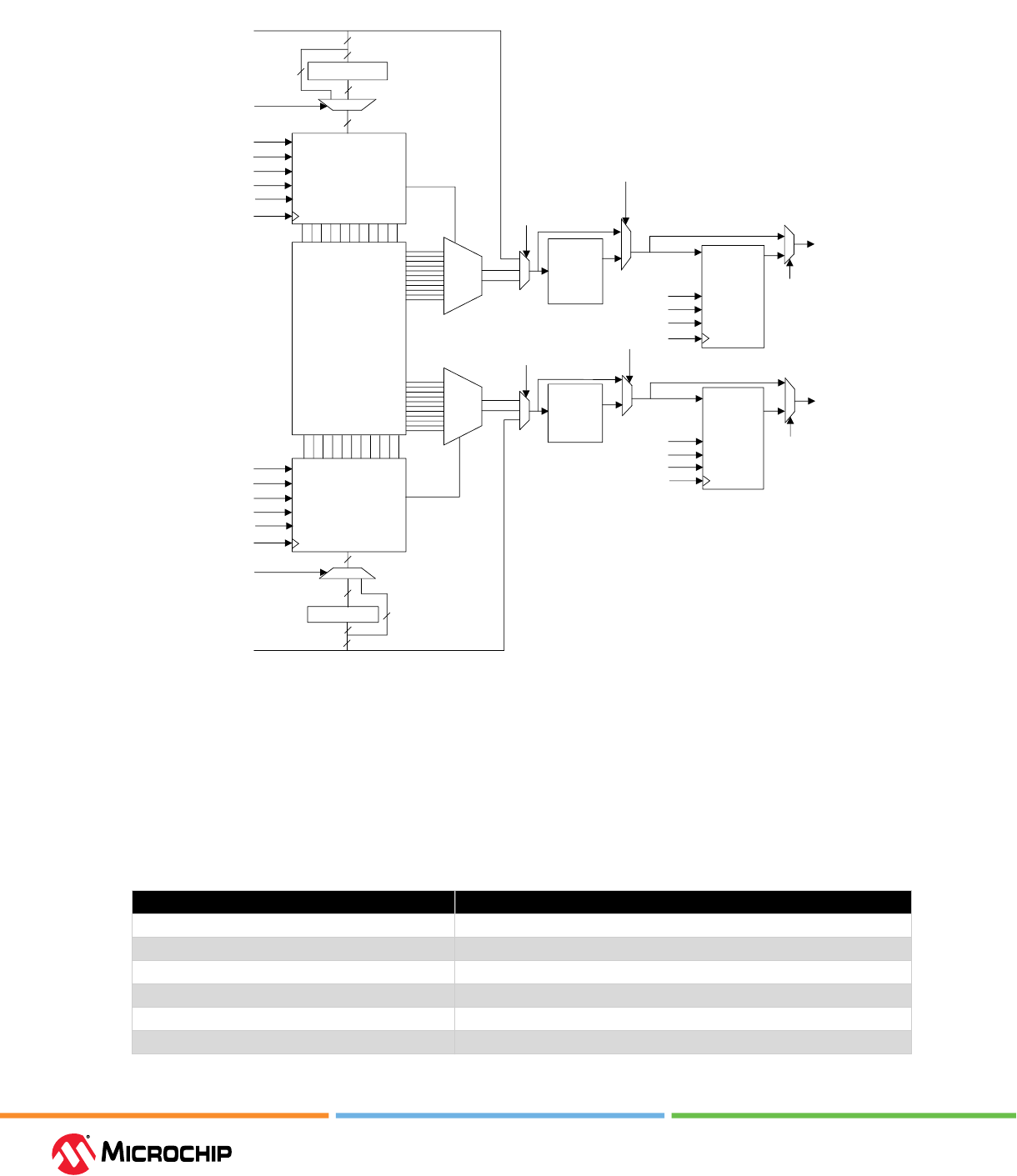
2.1.2 Two-Port Mode (Ask a Queson)
The LSRAM block can be congured as a Two-Port SRAM, where Port A is dedicated to read
operations and Port B is dedicated to write operations for data widths up to x20. For data widths
greater than x20, the read port borrows the unused Port B data output signals, similarly write port
borrows the unused Port A data input signals. Figure 2-8 shows the LSRAM in Two-Port mode with
independent write and read ports, pipeline registers, ECC logic, and feed-through MUXes to enable
immediate access to the write data. The ECC is supported only when the LSRAM is congured for
33-bit data width.
Embedded Memory Blocks
User Guide
© 2023 Microchip Technology Inc. and its subsidiaries
DS60001725G - 19
Figure 2-8. Simplied Funconal Block Diagram for LSRAM in Two-Port Mode
A_DOUT[19:0]*
A_DIN[19:0]*
B_DIN[19:0]*
A_ADDR[13:0]
A_WEN[1:0]
A_BLK_EN[2:0]
A_CLK
Port A Row Decode
Write Control
Port B Row Decode
Write Control
Column
Decode
Column
Decode
B_DOUT[19:0]*
Memory Array
B_DOUT_EN
B_DOUT_ARST_N
B_DOUT_SRST_N
A_DOUT_EN
A_DOUT_SRST_N
A_DOUT_ARST_N
B_CLK
A_CLK
20
Pipeline
Register A
Pipeline
Register B
A_WIDTH[2:0]
B_ADDR[13:0]
B_WEN[1:0]
B_BLK_EN[2:0]
ECC_EN
B_WIDTH[2:0]
ECC Encoder
20
ECC Encoder
ECC_EN
16 data and
4 ECC code bits
17 data and
3 ECC code bits
20
17
16
ECC
Decoder
+
Pipeline
Registers
ECC
Decoder
+
Pipeline
Registers
B_CLK
B_WMODE[1:0]
A_WMODE[1:0]
B_REN
A_REN
20
20
ECC_EN
ECC_EN
Note:
* For ECC mode:
A_DIN[15:0] and B_DIN[16:0]
A_DOUT[15:0] and B_DOUT[16:0]
20/17
A_BYPASS
B_BYPASS
2.1.2.1 Two-Port Data Width Conguraon (Ask a Queson)
In Two-Port mode, the maximum data width is x40. Each port can be congured in dierent data
widths. The conguration of read port has a corresponding conguration for the write port, as
shown in Table 2-6.
Table 2-6. LSRAM Data Width Conguraons (Two-Port Mode)
Read Port Write Port
x40 x5, x10, x20, x40
x20 x40
x10 x40
x5 x40
x2 x32
x1 x32
Embedded Memory Blocks
User Guide
© 2023 Microchip Technology Inc. and its subsidiaries
DS60001725G - 20
...........continued
Read Port Write Port
x33 x33
x32 x1, x2, x32
2.1.2.2 Byte Write Enables (Ask a Queson)
The byte write enables (A_WEN, B_WEN) enable writing individual bytes of data for x32, x33 and x40
data widths. For x40 width, the byte write enable for the corresponding data is used to enable each
of the four bytes; that is, byte write enable for Port A enables A_DIN[19:10] and A_DIN[9:0] and byte
write enable for Port B enables B_DIN[19:10] and B_DIN[9:0].
Table 2-7 lists the byte write enable settings for Port A and Port B.
Table 2-7. Byte Write Enable Sengs for Two-Port Mode
Depth x Width A_WEN/B_WEN Result
512 x 32 B_WEN[0] = 1 Write B_DIN[8:5], B_DIN[3:0]
B_WEN[1] = 1 Write B_DIN[18:15], B_DIN[13:10]
A_WEN[0] = 1 Write A_DIN[8:5], A_DIN[3:0]
A_WEN[1] = 1 Write A_DIN[18:15], A_DIN[13:10]
512 x 40 B_WEN[0] = 1 Write B_DIN[9:0]
B_WEN[1] = 1 Write B_DIN[19:10]
A_WEN[0] = 1 Write A_DIN[9:0]
A_WEN[1] = 1 Write A_DIN[19:10]
512 x 33 (with ECC Enabled) B_WEN[1:0] = 11
A_WEN[1:0] = 11
Write B_DIN[16:0]
Write A_DIN[15:0]
Important: For 512x32 conguration, bits 4, 9, 14, and 19 of data input ports are not used.
2.1.2.3 Read Enables (Ask a Queson)
The read enable signals, A_REN and B_REN, perform the read operation on ports A and B. When
read enable is low, the data outputs retain their previous state and no dynamic read power is
consumed on that port. When read enable is high, LSRAM performs read operation and consumes
read power.
Important: In Two-Port mode, LSRAM Port B read enable (B_REN) is tied to Port A read
enable (A_REN).
2.1.2.4 Pipeline Registers (Ask a Queson)
The outputs of the LSRAM have pipeline registers which can be enabled by the user for timing
closure. These pipeline registers can be reset synchronously or asynchronously as explained in the
following section.
2.1.2.4.1 Synchronous Pipeline Register Reset (Ask a Queson)
Each data output port has its own synchronous reset. In Two-Port mode, A_DOUT_SRST_N and
B_DOUT_SRST_N drive the synchronous reset of the read data output pipeline registers (A_DOUT
and B_DOUT). If the synchronous pipeline reset is low, the pipeline data output registers are reset to
zero on the next valid clock edge, as shown in the following gure.
Embedded Memory Blocks
User Guide
© 2023 Microchip Technology Inc. and its subsidiaries
DS60001725G - 21
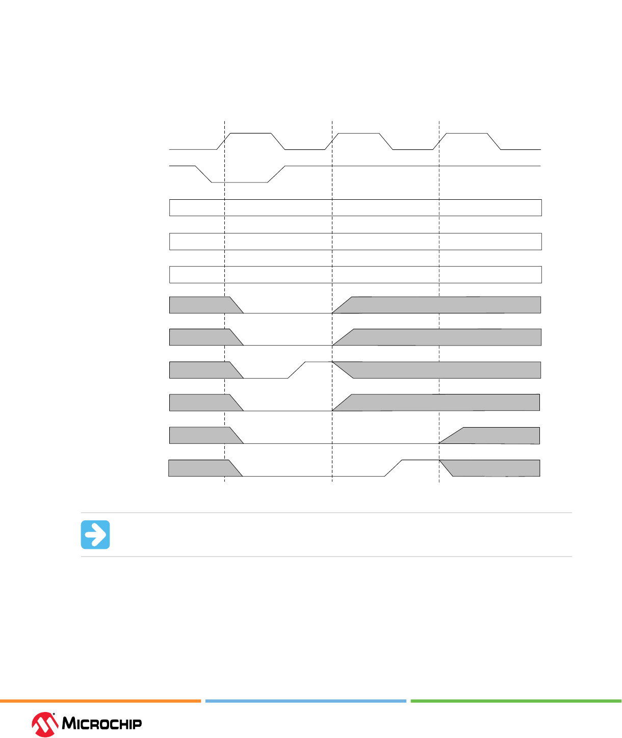
Figure 2-9. Synchronous Pipeline Reset in Two-Port Mode
A_CLK
B_CLK
A_DOUT_SRST_N
B_DOUT_SRST_N
A_DOUT[]
B_DOUT[]
SB_CORRECT
B_DETECT
A_DOUT[]
B_DOUT[]
SB_CORRECT
B_DETECT
Non-Pipeline Mode With/without ECC
Pipeline Mode with/without ECC
Clock Cycle #1 Clock Cycle #2
No Change
20'b0
Important: In x33 two-port mode, if ECC is in pipeline mode, this reset also resets the ECC
ag pipeline registers.
2.1.2.5 ECC Mode (For x33 Two-Port Mode Only) (Ask a Queson)
In the Two-Port mode, when the port width is set to x33, ECC (single-bit error correction and dual-bit
error detection) is available. The ECC encoder provides 40 bits (33 data bits and 7 encoded data
bits) of data in the x33 mode (the seven encoded bits are not accessible to the user). Single-bit and
dual-bit errors are counted for a full 33-bit read data word.
Important: ECC is supported only in two-port LSRAM congurations and not supported
for RTL inferred RAM blocks. For information about ECC conguration settings, see Figure
2-18.
The ECC decoder contains an optional pipeline register that adds a clock cycle of latency to the read
operation (including the ags). As the output data can also be pipelined, there are four possible
scenarios:
• Pipeline mode with non-pipelined ECC
• Pipeline mode with pipelined ECC
• Non-Pipeline mode with non-pipelined ECC
• Non-Pipeline mode with pipelined ECC
The following table lists the two ags generated by the ECC logic.
Table 2-8. Error Flags
ECC Errors SB_CORRECT DB_DETECT Correction
No error 0 0 NA
Single-bit error 1 0 Correction
Double-bit or Multi-bit error 1 1 No correction
Any multiple bit errors greater than one has both ags asserted, and the 33-bit read data word
not corrected. No scrubbing is done inside the LSRAM when ECC decoder detects any bit errors. All
scrubbing must be done in the fabric design. ECC simulation is not supported.

Embedded Memory Blocks
User Guide
© 2023 Microchip Technology Inc. and its subsidiaries
DS60001725G - 22
In the Pipeline mode, these ags are valid only in the read data output clock cycle. In Non-Pipeline
mode, the ECC ags are valid only in the same clock cycle as the corresponding read data output, as
the ags are reset in the next clock cycle.
In SmartDebug, the ECC bits are included in the 40 bits data divided between adjacent locations. 16
bits of data in one location and 17 bits of data in the next location, the remaining 5 bits are ECC
bits. The ECC bits are pre-calculated by Libero SoC and loaded in the background with the SRAM
initialization data. For information about loading the initializing client for the SRAM memory IP in
Libero SoC, see PolarFire Family Power-Up and Resets User Guide.
2.1.2.6 Read Operaon (Ask a Queson)
In two-port mode, LSRAM supports both pipelined and non-pipelined read operations. In a pipelined
read operation, the output data is registered at the pipeline registers making the data available
on the corresponding data output on the next clock cycle. If the ECC pipeline mode is enabled, an
additional clock cycle is required for read data output. ECC ags are valid in the same clock cycle as
the output data. For more information, see 2.1.2.5. ECC Mode (For x33 Two-Port Mode Only).
In non-pipelined read operations, the pipeline registers are bypassed and read data is available on
the output port in the same clock cycle. During this operation, LSRAM can generate glitches on
the data output buses. Therefore, it is recommended to use LSRAM with pipeline registers to avoid
glitches.
The following gure shows the timing for both pipelined and non-pipelined read operations in
two-port mode.
Embedded Memory Blocks
User Guide
© 2023 Microchip Technology Inc. and its subsidiaries
DS60001725G - 23
Figure 2-10. Read Operaon in Two-Port Mode
A_REN
B_REN
A_CLK
B_CLK
A_WEN[1:0]
B_WEN[1:0]
A_ADDR[]
B_ADDR[]
A_DOUT_EN
B_DOUT_EN
A_DOUT[]
B_DOUT[]
A_DOUT[]
B_DOUT[]
A_DOUT[]
B_DOUT[]
A_DOUT[]
B_DOUT[]
A_DOUT[]
B_DOUT[]
Non-Pipeline Mode with Non-Pipelined ECC
Non-Pipeline Mode without ECC
Pipeline Mode with Non-Pipelined ECC
Pipeline Mode with Pipelined ECC
Non-Pipeline Mode with Pipelined ECC
A0
A1 A2
Clock Cycle #1 Clock Cycle #2
D(A1)
D(A1)
D(A0)
D(A0)
D(A0)
SB_CORRECT
DB_DETECT
Non-Pipeline Mode with Non-Pipelined ECC
SB_CORRECT
DB_DETECT
Pipeline Mode with Non-Pipelined ECC
SB_CORRECT
DB_DETECT
Non-Pipeline Mode with Pipelined ECC
SB_CORRECT
DB_DETECT
Pipeline Mode with Pipelined ECC
Data in Address A0
D(A2)
D(A0)
D(A1)
D(A2)
D(A0)
D(A1)
Embedded Memory Blocks
User Guide
© 2023 Microchip Technology Inc. and its subsidiaries
DS60001725G - 24
2.1.2.7 Asynchronous Pipeline Register Reset (Ask a Queson)
Each data output port has its own asynchronous reset. In Two-Port mode, A_DOUT_ARST_N and
B_DOUT_SRST_N drive the asynchronous reset of the read data output pipeline registers (A_DOUT
and B_DOUT) and ECC pipeline registers. If the asynchronous pipeline reset is driven low, the
pipeline data output registers are immediately reset to zero, as shown in the following gure.
Figure 2-11. Asynchronous Pipeline Register Reset in Two-Port Mode
A_CLK
B_CLK
A_DOUT_ARST_N
B_DOUT_ARST_N
A_DOUT[19:0]
B_DOUT[19:0]
A_DOUT[15:0]
B_DOUT[16:0]
SB_CORRECT
B_DETECT
SB_CORRECT
DB_DETECT
A_DOUT[15:0]
B_DOUT[16:0]
SB_CORRECT
DB_DETECT
A_DOUT[15:0]
B_DOUT[16:0]
A_DOUT[15:0]
B_DOUT[16:0]
Pipeline Mode with Pipelined ECC
Pipeline Mode with Pipelined ECC
Pipeline Mode with Non-Pipelined ECC
Non-Pipeline Mode with Pipelined ECC
Non-Pipeline Mode with Pipelined ECC
Pipeline Mode without ECC
Non-Pipeline Mode with Non-Pipelined ECC
Non-Pipeline Mode with Non-Pipelined ECC
Non-Pipeline Mode without ECC
Clock Cycle #1 Clock Cycle #2
A_DOUT[19:0]
B_DOUT[19:0]
20'b0
Important: In x33 Two-Port mode, if ECC is in pipeline mode, then this reset also resets
the ECC ag pipeline registers.
2.1.3 Implementaon (Ask a Queson)
An LSRAM block is implemented in a design using the following methods:
• 2.1.3.1. RTL Inference during Synthesis
• 2.1.3.2. LSRAM Congurator
• 2.1.3.3. LSRAM Memory Macro

Embedded Memory Blocks
User Guide
© 2023 Microchip Technology Inc. and its subsidiaries
DS60001725G - 25
2.1.3.1 RTL Inference during Synthesis (Ask a Queson)
Synplify Pro ME can infer an LSRAM from RTL automatically based on memory logic used in the
design. In this case, synthesis handles all the signal connections of the LSRAM block to the rest of
the design and sets the correct values for the static signals needed to congure the appropriate
operational mode. The tool ties unused dynamic input signals to ground and provides default values
to unused static signals. If a design requires more memory blocks than the blocks available in the
device, the Synthesis tool will infer fabric registers for the extra memory blocks.
For more information about LSRAM inference by Synplify Pro, see Inferring PolarFire RAM Blocks
Application Note.
2.1.3.2 LSRAM Congurator (Ask a Queson)
The Libero SoC software catalog has the following LSRAM conguration tools:
• 2.1.3.2.1. Dual-Port Large SRAM Congurator
• 2.1.3.2.2. Two-Port LSRAM Congurator
Using these congurators, the LSRAM can be congured as per design requirements. The generated
LSRAM component can be instantiated in the SmartDesign. The congurators generate the HDL
wrapper les for LSRAM with the appropriate values assigned to the static signals. Use the
generated HDL wrapper les in the design hierarchy by connecting the ports to the rest of the
design.
2.1.3.2.1 Dual-Port Large SRAM Congurator (Ask a Queson)
The PF_DPSRAM congurator is available in the Libero SoC IP Catalog > Memory & Controllers.
The PF_DPSRAM congurator automatically cascades LSRAM blocks to create wider and deeper
memories by selecting the most ecient aspect ratio. It also handles the grounding of unused
bits. The congurator supports the generation of memories that have dierent aspect ratios on
each port. The congurator uses one or more memory blocks to generate a RAM to match the
conguration. The congurator also creates an external logic required for the cascading.
The congurator cascades RAM blocks in three dierent methods:
• Cascaded deep—For example, two blocks of 16384 x 1 are combined to create a 32768 x 1.
• Cascaded wide—For example, two blocks of 16384 x 1 are combined to create a 16384 x 2.
• Cascaded wide and deep—For example, four blocks of 16384 x 1 are combined to create a 32768
x 2, in a two-block width by two-block depth conguration.
For more information on Dual-Port mode, see 2.1.1. Dual-Port Mode.
Embedded Memory Blocks
User Guide
© 2023 Microchip Technology Inc. and its subsidiaries
DS60001725G - 26
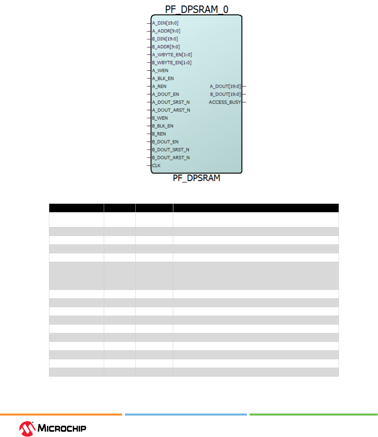
Figure 2-12. Dual-Port Large SRAM Congurator: Generated Component
Table 2-9. Dual-Port LSRAM Congurator Signals
Port Direction Polarity Description
CLK Input Rising edge Single-clock signal that drives both ports with the same clock. Exposed
only when single clock is selected.
A_DIN[19:0] Input — Port A write data
A_ADDR[9:0] Input — Port A read address
A_BLK_EN Input Active High Port A block select
A_CLK Input Rising edge Port A clock. Applicable only when independent clocks are selected.
A_WEN Input — Port A signal to switch between write and read modes:
• Low: Read
• High: Write
A_REN Input — Port A read data enable
A_WBYTE_EN[1:0] Input — Port A write byte enable
A_DOUT[19:0] Output — Port A read data
A_DOUT_EN Input Active High Port A read data register enable
A_DOUT_SRST_N Input Active Low Port A read data register synchronous reset
A_DOUT_ARST_N Input Active Low Port A read data register asynchronous reset
B_DIN[19:0] Input — Port B write data
B_ADDR[9:0] Input — Port B address
B_BLK_EN Input Active High Port B enable
B_CLK Input Rising edge Port B clock. Applicable only when independent clocks are selected
Embedded Memory Blocks
User Guide
© 2023 Microchip Technology Inc. and its subsidiaries
DS60001725G - 27
...........continued
Port Direction Polarity Description
B_WEN Input — Port signal to switch between write and read modes:
• Low: Read
• High: Write
B_REN Input — Port B read data enable
B_WBYTE_EN[1:0] Input — Port B write byte enable
B_DOUT[19:0] Output — Port B read data
B_DOUT_EN Input Active High Port B read data register enable
B_DOUT_SRST_N Input Active Low Port B read data register synchronous reset
B_DOUT_ARST_N Input Active Low Port B read data register asynchronous reset
ACCESS_BUSY Output Active High Busy signal when being initialized or accessed using SmartDebug
The dual-port LSRAM congurator has three tabs:
• Parameter settings
• Port settings
• Memory initialization
Parameter Settings
The parameter settings include the optimization of LSRAM for High Speed or Low Power, clock signal
settings, and optional port settings. The following gure shows the Dual-Port Large LSRAM block
congurator.
Figure 2-13. Dual-Port Large SRAM Congurator: Parameter Sengs
Optimization for High Speed or Low Power
You can optimize the LSRAM with one of the following options:
• High Speed—Optimizes the LSRAM for speed and area by using width cascading.
Embedded Memory Blocks
User Guide
© 2023 Microchip Technology Inc. and its subsidiaries
DS60001725G - 28
• Low Power—Optimizes the LSRAM for low power by using depth cascading, it uses additional
logic at the input and output.
Single Clock (CLK) or Independent Clocks (A_CLK and B_CLK)
You can set the clock signals and the signal polarity:
• Single clock—Drives both A and B ports with the same clock. This is the default conguration for
dual-port LSRAM.
• Independent clocks—Selects independent clock for each A_CLK for Port A and B_CLK for Port B).
• Rising edge or Falling edge—Changes the signal polarity.
Optional Ports
You can select one of the following optional ports:
• Lock access to SmartDebug—When enabled, SmartDebug access to the RAM is disabled.
• Expose ACCESS_BUSY output—When enabled, SmartDebug ACCESS_BUSY signal is available as
top-level port.
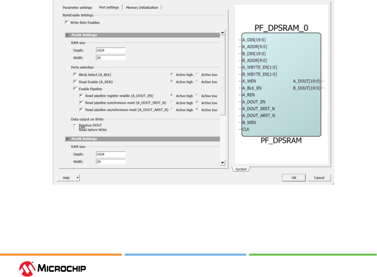
Port Settings
In the Port Settings tab, you can set the RAM size, select ports, and set data output on write settings
for both Ports A and B. The following gure shows the PF_DPSRAM block port settings.
Figure 2-14. Dual-Port Large SRAM Congurator: Port Sengs
Byte Enable Settings
Write Byte Enables—Enables writing to individual bytes of data (A_WBYTE_EN and B_WBYTE_EN).
The Write Byte Enable bits are all the control signals exposed by each column of LSRAM blocks when
the implementation splits the word width. The LSRAM congurator generates the most ecient
conguration of the depth and width for high-speed or low-power selection. Depending on the
Embedded Memory Blocks
User Guide
© 2023 Microchip Technology Inc. and its subsidiaries
DS60001725G - 29
generated conguration, each Write Byte Enable bit may control up to 10 bits of data. In other
words, the Write Byte Enable option does not govern the implementation.
In low-power mode for word widths that are multiples of 8, each Write Byte Enable bit controls 8 bits
unless the word width is also a multiple of 10. For example, generating a 32-bit word width LSRAM,
with Write Byte Enables, cascades the RAMs width-wise such that there are a total of 4 Write Byte
Enable bits (2 per RAM block) and each Write Byte Enable bit controls the writing of 8-bits of data.
Other Examples are as follows:
• Width of 17, is divided as 9 + 8.
• Width of 35, is rst divided as 18 + 17, and then, divided as 9 + 9 + 9 + 8.
RAM Size
You can set the RAM size.
• Depth—Sets the depth range. The depth range for each port is between 1 and 524288. The
maximum value depends on the die.
• Width—Sets the width range. The width range for each port is between 1 and 19040.
Important: The two ports can be congured independently for any depth and width.
However, Port A depth x Port A width must be equal to Port B depth x Port B width. The
width range varies between devices.
Ports Selection: Block Select (A_BLK_EN and B_BLK_EN)
The default conguration for A_BLK_EN and B_BLK_EN is unchecked, which ties the signal to the
Active state and removes it from the generated component. Select Active high or Active low to
change the signal polarity. Ports are populated on the component by checking the respective check
boxes.
Read Enable (A_REN and B_REN)
The default conguration for A_REN or B_REN is unchecked, which ties the signal to the active state
and removes it from the generated macro. Select Active high or Active low to change the signal
polarity. Ports are populated on the component by checking the respective check boxes.
Enable Pipeline
Check the Enable Pipeline check box to enable pipelining of read data (A_DOUT or B_DOUT).
If the Enable Pipeline check box is disabled, you cannot congure the A_DOUT_EN/B_DOUT_EN,
A_DOUT_SRST_N/B_DOUT_SRST_N, or A_DOUT_ARST_N/B_DOUT_ARST_N signals.
• Register Enable (A_DOUT_EN and B_DOUT_EN)—the pipeline registers for ports A and B have
active-high, enable inputs. By default, the check box is disabled. Selecting this check box adds the
signal to the top-level port.
• Synchronous Reset (A_DOUT_SRST_N and B_DOUT_SRST_N)—the pipeline registers for ports A
and B have active-low, synchronous reset inputs. By default, the check box is disabled. Selecting
this check box adds the signal to the top-level port.
• Asynchronous Reset (A_DOUT_ARST_N and B_DOUT_ARST_N)—the pipeline registers for ports
A and B have active-low, asynchronous reset inputs. By default, the check box is disabled.
Selecting this check box adds the signal to the top-level port.
Select Active high or Active low to change the signal polarity. Ports are populated on the
component by checking their respective check boxes.
Data Output on Write
Select the required option from the following:
Embedded Memory Blocks
User Guide
© 2023 Microchip Technology Inc. and its subsidiaries
DS60001725G - 30
• Previous DOUT—The default data on the Read data output (A_DOUT or B_DOUT) during a write
cycle is the DOUT data from the previous cycle (Previous DOUT).
• DIN—To enable feed-through write mode on Read data output.
• Read before Write—To perform a read operation before a write operation overwriting the
previous data.
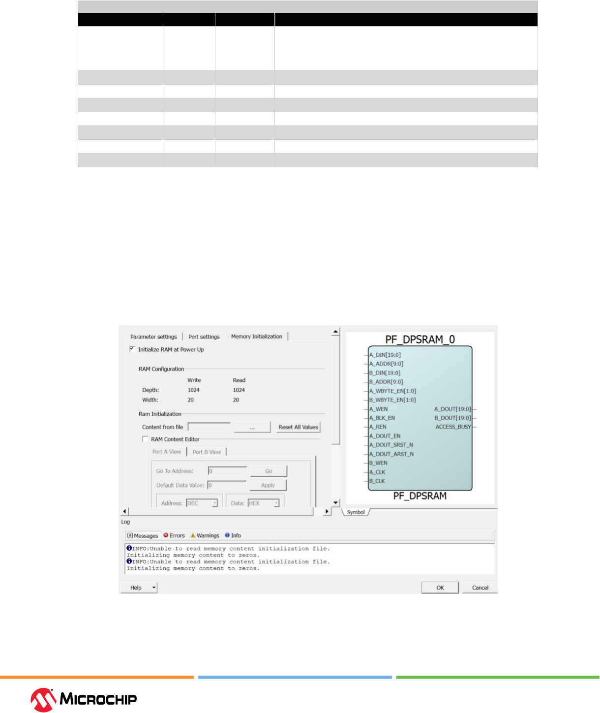
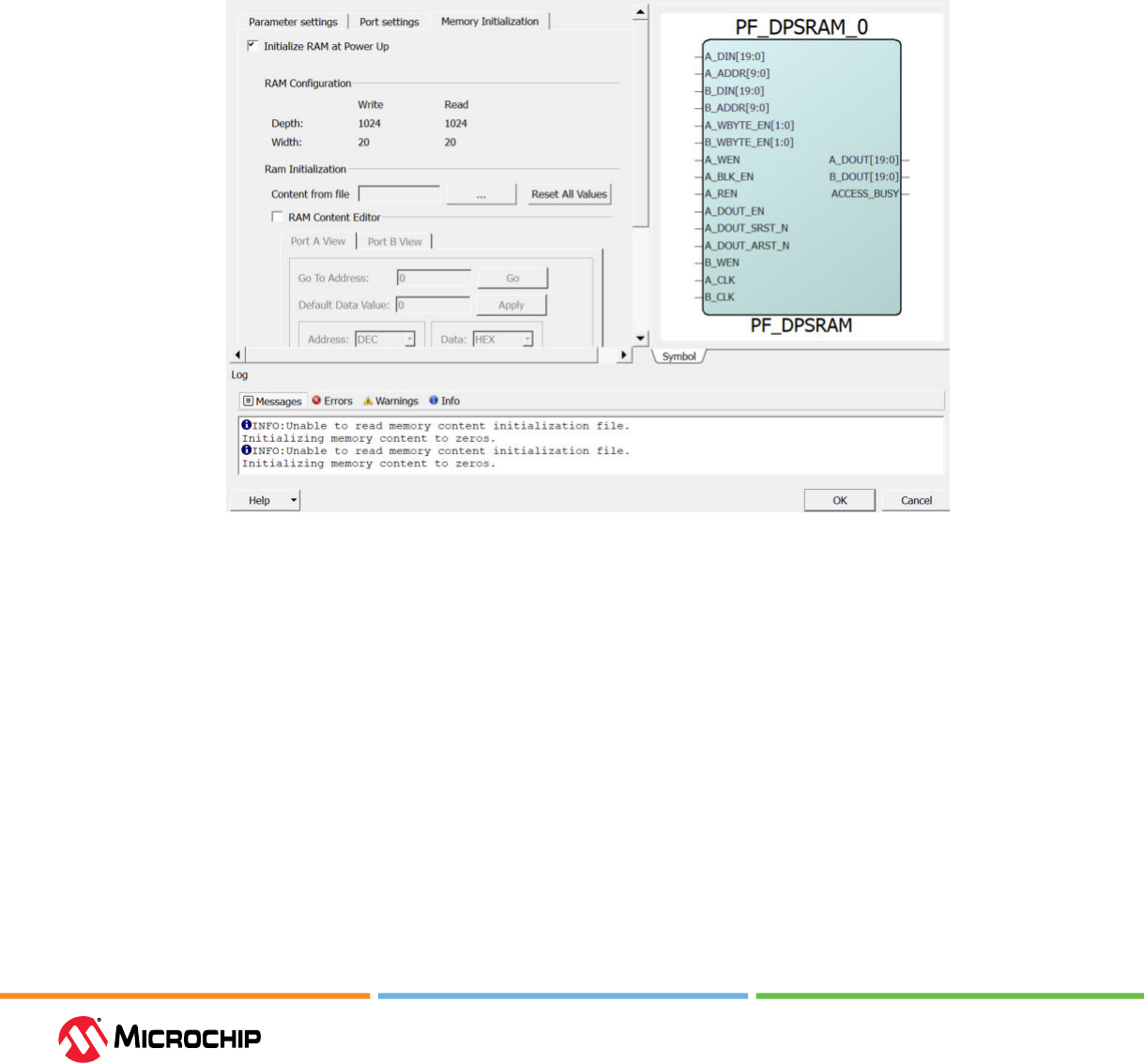
Memory Initialization at Power-Up
In the Memory Initialization tab, you can initialize RAM at power-up. LSRAM can be initialized
during device power-up and functional simulation. The following gure shows the PF Dual Port Large
SRAM IP memory initialization.
Figure 2-15. Dual-Port Large SRAM Congurator: Memory Inializaon
Initialize RAM at Power Up
You can initialize RAM during power-up of the device by setting the following:
• Initialize RAM at Power Up—Loads the RAM content during device operation at power-up and
functional simulation.
• RAM Conguration—Both write and read depths and widths are displayed as specied in the
Port settings tab.
• Initialize RAM Contents From File—The RAM’s content can be initialized by importing the
memory le. This avoids the simulation cycles required for initializing the memory and reduces
the simulation runtime. The congurator partitions the memory le appropriately so that the
right content goes to the right block RAM when multiple blocks are cascaded.
• Import File—Selects and imports a memory content le (Intel-Hex) from the Import Memory
Content dialog box. File extensions are set to *.hex for Intel-Hex les during import. For more
information, see 4. Appendix: Supported Memory File Formats for LSRAM and μSRAM. The
imported memory content is displayed in the RAM Content Editor.
• Reset All Values—Resets all the data values. This option is enabled when the RAM Content
Editor check box is selected.

Embedded Memory Blocks
User Guide
© 2023 Microchip Technology Inc. and its subsidiaries
DS60001725G - 31
RAM Content Editor
The RAM Content Editor enables the user to specify the contents of RAM memory manually for both
Port A and Port B. It also allows you to modify imported data.
Port A View/Port B View
• Go To Address—Enables you to go to a specic address in the editor. You can select the number
display format (HEX, BIN, and DEC) from the Address menu.
• Default Data Value—You can set this with new data to change the default. When the data value
is changed, all default values in the manager are updated to match the new value. You can select
the number display format (HEX, BIN, and DEC) from the Data menu.
• Address—The Address column lists the address of a memory location. The menu species the
number format of the address list (hexadecimal, binary, or decimal).
• Data—Controls the data format and data values in the manager.
Click OK to close the manager and save all changes made to the memory and its contents. Click
Cancel to close the manager and cancel all the changes.
Important: The dialogs show all data with the MSb down to LSb. For example, if the row
showed 0xAABB for a 16-bit word size, the AA is MSb and BB is LSb.
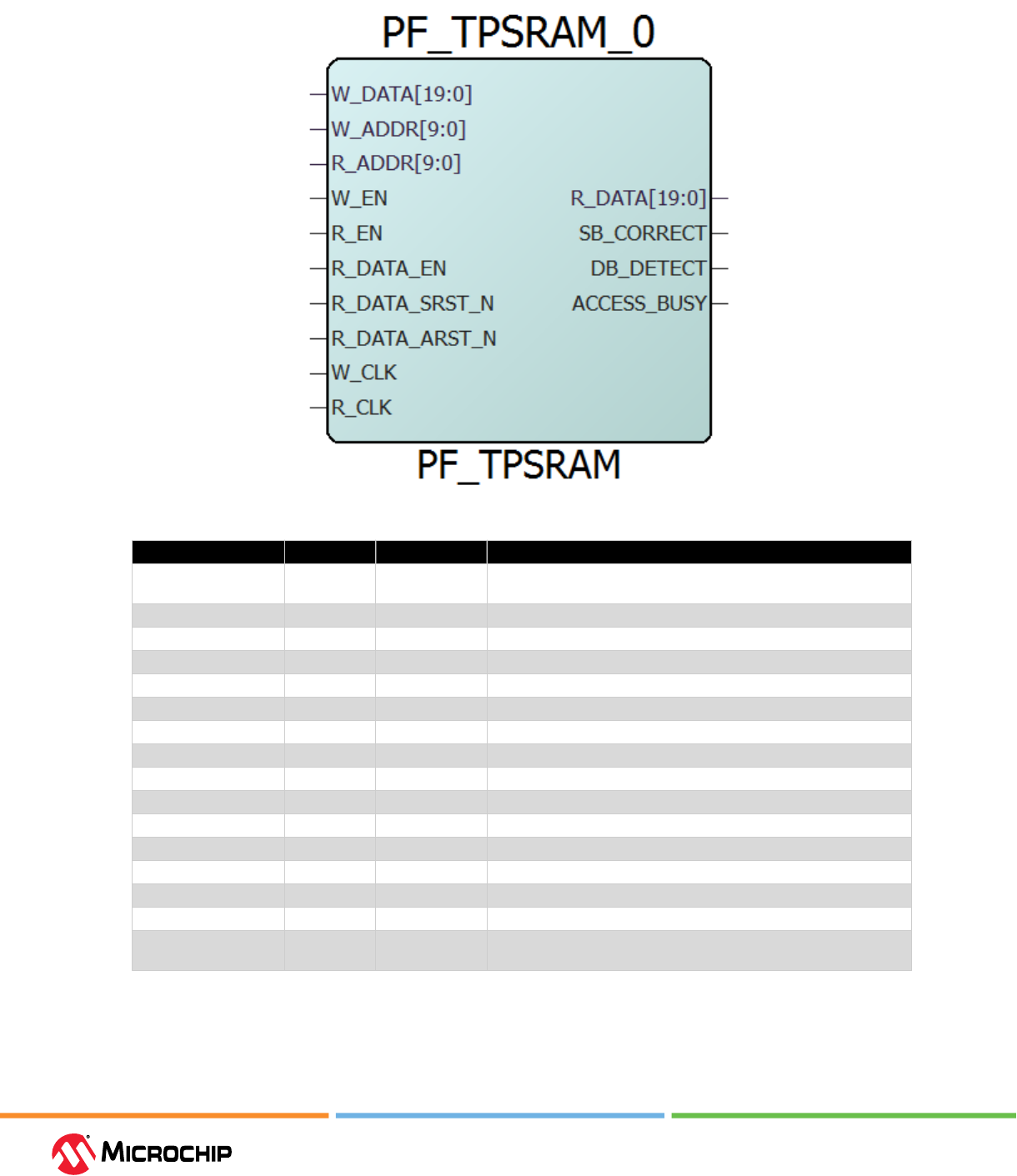
2.1.3.2.2 Two-Port LSRAM Congurator (Ask a Queson)
The Two-Port SRAM (TPSRAM) IP congurator is available in the Libero SoC software under Memory
& Controllers. The following gure shows the TPSRAM IP block available in the Libero SoC software.
The TPSRAM congurator enables write access on one port and read access on the other port. The
RAM congurator automatically cascades LSRAM blocks to create wider and deeper memories by
selecting the most ecient aspect ratio. It also handles the grounding of unused bits. The core
congurator supports the generation of memories that have dierent write and read aspect ratios.
The congurator uses one or more memory blocks to generate a RAM matching the conguration. In
addition, it also creates the surrounding cascading logic.
The congurator cascades RAM blocks in three dierent methods:
• Cascaded deep—For example, two blocks of 16384 x 1 combined to create a 32768 x 1.
• Cascaded wide—For example, two blocks of 16384 x 1 combined to create a 16384 x 2.
• Cascaded wide and deep—For example, four blocks of 16384 x 1 combined to create a 32768 x 2,
in two blocks width-wise by two blocks depth-wise conguration.
Embedded Memory Blocks
User Guide
© 2023 Microchip Technology Inc. and its subsidiaries
DS60001725G - 32
Figure 2-16. Two-Port Large SRAM Congurator with ECC Enabled
Table 2-10. Two-Port Large SRAM Congurator Signals
Port Direction Polarity Description
CLK Input Rising edge Single clock to drive both W_CLK and R_CLK. Applicable only when
single read/write clock is selected.
W_DATA[19:0] Input — Write data
W_ADDR[9:0] Input — Write address
W_EN Input Active High Write port enable
W_CLK Input Rising edge Write clock. Applicable only when independent clocks are selected.
R_CLK Input Rising edge Read clock. Applicable only when independent clocks are selected.
R_EN Input Active High Read data enable.
WBYTE_EN[] Input — Write enable for byte write.
R_ADDR[9:0] Input — Read address
R_DATA[19:0] Output — Read data
R_DATA_EN Input Active High Read data register enable
R_DATA_SRST_N Input Active Low Read data register synchronous reset
R_DATA_ARST_N Input Active Low Read data register asynchronous reset
SB_CORRECT Output Active High Single-bit correct ag. Applicable only when ECC is enabled.
DB_DETECT Output Active High Double-bit detect ag. Applicable only when ECC is enabled.
ACCESS_BUSY Output Active High Busy signal from SmartDebug. Exposed only when Expose
ACCESS_BUSY output is checked.
The Two-Port LSRAM congurator has three tabs:
• Parameter settings
• Port settings
Embedded Memory Blocks
User Guide
© 2023 Microchip Technology Inc. and its subsidiaries
DS60001725G - 33
• Memory initialization settings
Parameter Settings
The parameter settings include the Optimization for High Speed or Low Power, clock signals settings,
and optional port settings. The following gure shows the TPSRAM block congurator.
Figure 2-17. Two-Port Large SRAM Congurator: Parameter Sengs
Optimization for High Speed or Low Power
You can optimize the LSRAM macro with one of the following options:
• High Speed—Optimizes the LSRAM macro for speed and area by using width cascading.
• Low Power—Optimizes the LSRAM macro for low power, but it uses additional logic at the input
and output by using depth cascading.
Single Read/Write Clock (CLK) or Independent Read/Write Clocks
You can set the clock signals and the signal polarity as follows:
• Single clock—Drives write and read with the same clock. This is the default conguration for
Two-Port LSRAM.
• Independent clocks—Selects independent clock for Read (R_CLK) and Write (W_CLK)—R_CLK
and W_CLK.
• Rising edge or Falling edge—Sets the signal polarity.
Optional Ports
The user can select one of the following optional ports:
• Lock access to SmartDebug—When enabled, SmartDebug access to the RAM is disabled.
• Expose ACCESS_BUSY output—When enabled, SmartDebug ACCESS_BUSY signal is available as
top-level port.
Embedded Memory Blocks
User Guide
© 2023 Microchip Technology Inc. and its subsidiaries
DS60001725G - 34
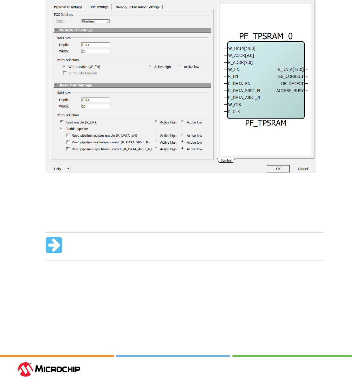
Port Settings
In the Port Settings tab, the user can set RAM size, select ports, and set data output on write
settings for both ports. The following gure shows the TPSRAM block port settings.
Figure 2-18. Two-Port Large SRAM Congurator: Port Sengs
ECC
The following three Error Correction Code (ECC) options are available:
• Disabled
• Pipelined
• Non-pipelined
Important: When ECC is enabled (pipelined or non-pipelined), both ports have data
widths equal to 33 bits. The SB_CORRECT and DB_DETECT output ports are exposed when
ECC is enabled.
Write Byte Enable Settings
Write Byte Enables—Enables the writing of individual bytes of data (WBYTE_EN). This port is
disabled while the ECC is enabled.
The Write Byte Enable bits are all the control signals exposed by each column of LSRAM blocks when
the implementation splits the word width. The LSRAM congurator generates the most ecient
conguration of the depth and width for high-speed or low-power selection. Depending on the
generated conguration, each Write Byte Enable bit may control up to 10 bits of data. In other
words, the Write Byte Enable option does not govern the implementation.

Embedded Memory Blocks
User Guide
© 2023 Microchip Technology Inc. and its subsidiaries
DS60001725G - 35
In low-power mode for word widths that are multiples of 8, each Write Byte Enable bit will control
8 bits unless the word width is also a multiple of 10. For example, generating a 32-bit word width
LSRAM, with Write Byte Enables, will cascade the RAMs width-wise such that there are a total of 4
Write Byte Enable bits (2 per RAM block) and each Write Byte Enable bit controls the writing of 8-bits
of data.
Other examples are as follows:
• Width of 17, is divided as 9 + 8.
• Width of 35, is rst divided as 18 + 17, and then, divided as 9 + 9 + 9 + 8.
RAM Size
You can set the RAM size using the following options.
• Depth—Sets the depth range. The depth range for each port is between 1 and 524288. The
maximum value depends on the die.
• Width—Sets the width range. The width range for each port is between 1 and 38080.
Important: The two ports can be congured independently for any depth and width. The
write port depth x write port width must be equal to read port depth x read port width. The
width range varies for dierent devices. The performance of the RAM is aected if width
and depth are too large.
Write Enable (W_EN)—The default conguration for W_EN is checked (enabled). Clearing the W_EN
option ties the signal to the Active state and removes it from the generated macro. Use Active high
or Active low to change the signal polarity.
Read Enable (R_EN)—The default conguration for R_EN is unchecked (disabled), which ties the
signal to the Active state and removes it from the generated macro. Selecting the check box enables
R_EN and the associated functionality. Use Active high or Active low to change the signal polarity.
Important: You can insert the signal on the generated macro by checking its respective
check boxes.
Enable Pipeline
Select the Enable Pipeline check box to enable pipelining of Read data (R_DATA). This is a static
selection and cannot be changed dynamically by driving it with a signal. If the Enable Pipeline
check box is not checked, the user cannot congure R_DATA_EN, R_DATA_SRST_N, or R_DATA_ARST_N
signals.
• Read Pipeline Register Enable (R_DATA_EN)—The pipeline registers for R_DATA have an active
high, enable input. By default, the check box is disabled. Selecting this check box adds the signal
to the top-level port.
• Read Pipeline Synchronous Reset (R_DATA_SRST_N)—The pipeline registers for R_DATA have an
active-low, synchronous reset input. By default, the check box is disabled. Selecting this check box
adds the signal to the top-level port.
• Read Pipeline Asynchronous Reset (R_DATA_ARST_N)—The pipeline registers for R_DATA have
an active-low, asynchronous reset input. By default, the check box is disabled. Selecting this check
box adds the signal to the top-level port.
• Active high or Active low—sets the signal polarity.
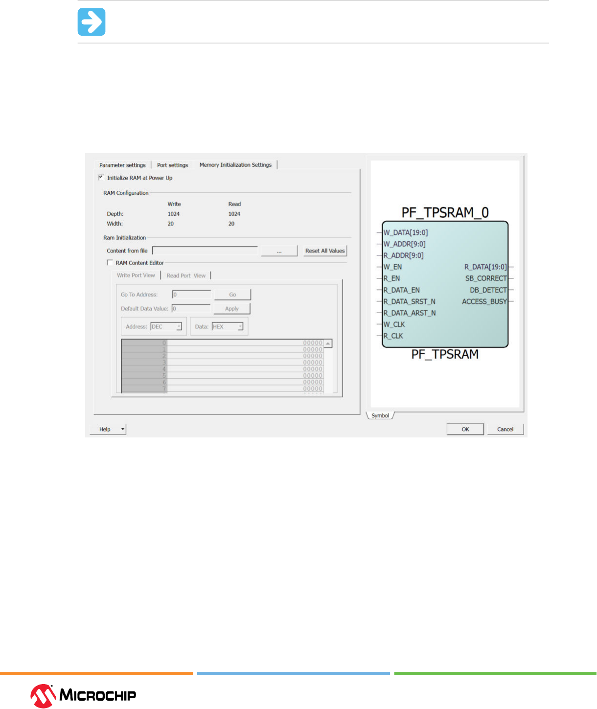
Embedded Memory Blocks
User Guide
© 2023 Microchip Technology Inc. and its subsidiaries
DS60001725G - 36
Important: You can insert the signal on the generated macro by checking the respective
check boxes.
Memory Initialization at Power-Up
In the Memory Initialization tab, the user can initialize RAM at power-up. LSRAM can be initialized
during device power-up and functional simulation as described in Memory Initialization at Power-
Up of 2.1.3.2.1. Dual-Port Large SRAM Congurator. The following gure shows the TPSRAM IP
memory initialization.
Figure 2-19. Two-Port Large SRAM Congurator: Memory Inializaon
The Reset All Values option resets all the data values. This option is enabled when the RAM
Content Editor check box is selected.
2.1.3.3 LSRAM Memory Macro (Ask a Queson)
An LSRAM primitive is available as a component that can be used directly in the HDL le or
instantiated in SmartDesign. For more information about conguring LSRAM, see 5.1. LSRAM
Macro.
2.2 μSRAM (Ask a Queson)
Each μSRAM has one read port and one write port for Two-Port memory requirements. The
following gure shows the μSRAM I/O diagram.
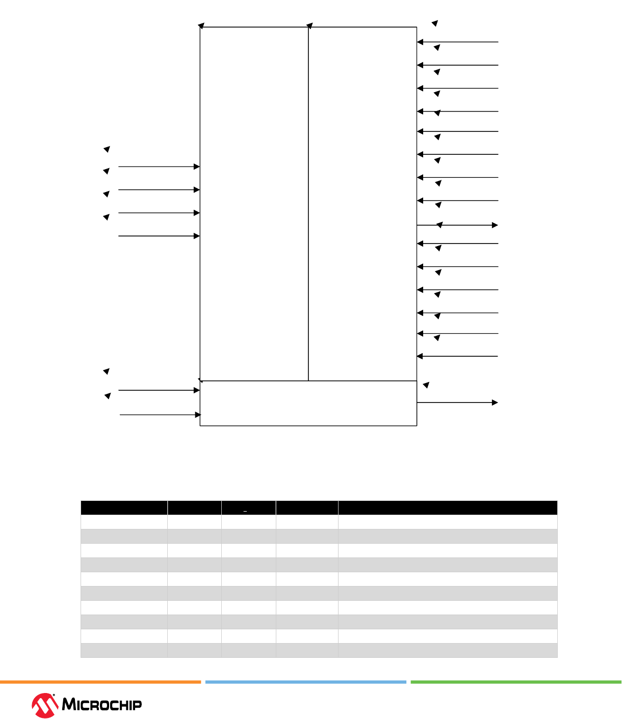
Embedded Memory Blocks
User Guide
© 2023 Microchip Technology Inc. and its subsidiaries
DS60001725G - 37
Figure 2-20. µSRAM Input/Output
Common Signals
Write Port Read Port
W_ADDR[5:0]
W_CLK
W_DATA[11:0]
W_EN
R_ADDR[5:0]
R_ADDR_AD_N
R_ADDR_AL_N
R_ADDR_BYPASS
R_ADDR_EN
R_ADDR_SD
R_ADDR_SL_N
R_CLK
R_DATA[11:0]
R_DATA_AD_N
R_DATA_AL_N
R_DATA_BYPASS
R_DATA_EN
R_DATA_SD
R_DATA_SL_N
ACCESS_BUSY
BLK_EN
BUSY_FB
The following table lists the ports available in μSRAM.
Table 2-11. Port List for μSRAM
Pin Name Direction Type
1
Polarity Description
W_EN Input Dynamic Active High Write enable
W_CLK Input Dynamic Rising edge Write clock
W_ADDR[5:0] Input Dynamic — Write address
W_DATA[11:0] Input Dynamic — Write-data
BLK_EN Input Dynamic Active High Read port enable
R_CLK Input Dynamic Rising edge Read clock
R_ADDR[5:0] Input Dynamic — Read-address
R_ADDR_BYPASS Input Static Active High Read-address and BLK_EN bypassed when High
R_ADDR_EN Input Dynamic Active High Read-address register Enable
R_ADDR_SL_N Input Dynamic Active Low Read-address register synchronous load
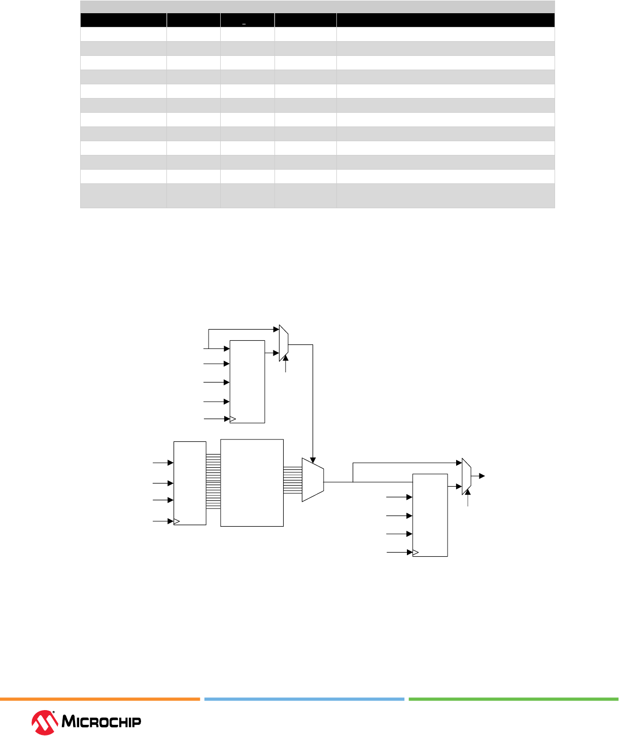
Embedded Memory Blocks
User Guide
© 2023 Microchip Technology Inc. and its subsidiaries
DS60001725G - 38
...........continued
Pin Name Direction Type
1
Polarity Description
R_ADDR_SD Input Static Active High Read-address register synchronous load data
R_ADDR_AL_N Input Dynamic Active Low Read-address register asynchronous load
R_ADDR_AD_N Input Static Active Low Read-address register asynchronous load data
R_DATA[11:0] Output Dynamic — Read-data
R_DATA_BYPASS Input Static Active High Read-data pipeline register bypassed when High
R_DATA_EN Input Dynamic Active High Read-data pipeline register enable
R_DATA_SL_N Input Dynamic Active Low Read-data pipeline register synchronous load
R_DATA_SD Input Static Active High Read-data pipeline register synchronous load data
R_DATA_AL_N Input Dynamic Active Low Read-data pipeline register asynchronous load
R_DATA_AD_N Input Static Active Low Read-data pipeline register asynchronous load data
BUSY_FB Input Static Active High Lock access to SmartDebug
ACCESS_BUSY Output Dynamic Active High Busy signal when the RAM is being initialized or
accessed using SmartDebug
Note:
1. Static inputs are tied to 0 or 1 during design implementation.
The following gure shows the μSRAM with independent write and read ports and read data pipeline
registers.
Figure 2-21. Simplied Funconal Block Diagram of µSRAM
Write
Control
Memory Array
64x12
Read
Decod
e
R_DATA[11:0]
R_DATA_EN
W_CLK
Read
Data
Pipeline
Register
R_DATA_AL_N
R_DATA_AD_N
R_CLK
W_ADDR[5:0]
W_DATA[11:0]
W_EN
R_ADDR_EN
Read
Address
Pipeline
Register
R_ADDR_AL_N
R_ADDR_AD_N
R_CLK
R_ADDR[5:0]
R_DATA_BYPASS
R_ADDR_BYPASS
2.2.1 Read Operaon (Ask a Queson)
Read operations are independent of write operations and are performed asynchronously.
Synchronous read operations can be performed by using fabric ip-ops as pipeline registers. These
ip-ops are located in the associated interface cluster at the read address input and read data
output.
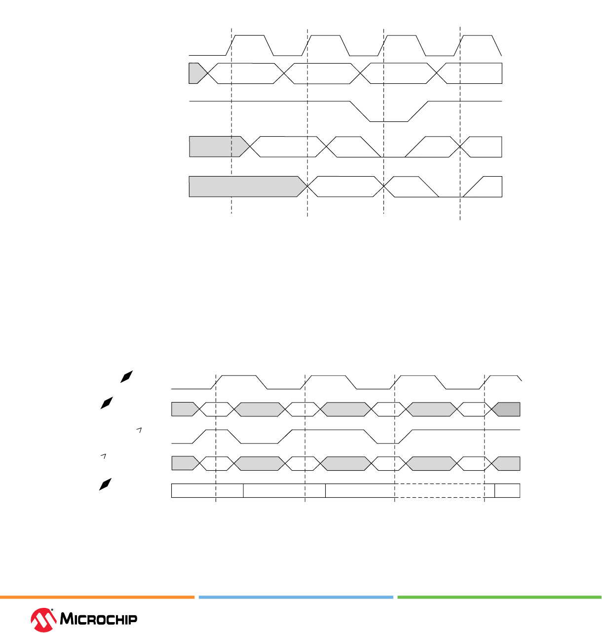
Embedded Memory Blocks
User Guide
© 2023 Microchip Technology Inc. and its subsidiaries
DS60001725G - 39
When the input address (R_ADDR[]) is provided, the output data is available on the output data
bus. When BLK_EN is high, the read operations are enabled. R_DATA contains the contents of the
memory location selected by R_ADDR. When BLK_EN is low, the R_DATA is driven to zero.
The following gure shows the timing of read operation.
Figure 2-22. Read Operaon in µSRAM
R_ADDR[5:0]
BLK_EN
R_DATA[11:0]
A0
A1
A2
D(A1)
D(A2)
A3
D(A0)
D(A3)
R_CLK
Clock Cycle #1 Clock Cycle #2 Clock Cycle #3
R_DATA[11:0]
D(A1)
D(A2)
D(A0)
Pipelined Mode
Non- Pipelined Mode
20'b0
20'b0
2.2.2 Write Operaon (Ask a Queson)
μSRAM supports synchronous write operation. The write port inputs are registered on the rising
edge of the write port clock, W_CLK.
When write enable (W_EN) is high, the data (W_DATA) is written to the RAM at the address (W_ADDR)
after write delay. When the write enable (W_EN) is low, no write operation is performed.
Figure 2-23. Write Operaon in µSRAM
W_DATA[11:0]
W_EN
W_CLK
W_ADDR[5:0]
Data written
to µSRAM
D0
D1
D2 D3
No Write
D0
D1
D3
A0
A1
A2 A3
Clock Cycle #1 Clock Cycle #2 Clock Cycle #3

Embedded Memory Blocks
User Guide
© 2023 Microchip Technology Inc. and its subsidiaries
DS60001725G - 40
2.2.3 Collision (Ask a Queson)
Collision occurs when write and read-write operations requested for the same address at the
same time. Simultaneous write and read operations at the same location are not supported. In
μSRAM, collision is not supported and write operations supersede read operations. Therefore,
during collision the read operation generates invalid data at the output until the write operation
is completed.
2.2.4 Implementaon (Ask a Queson)
An μSRAM block can be implemented in a design by the following methods:
• 2.2.4.1. RTL Inference during Synthesis
• 2.2.4.2. μSRAM Congurator
• 2.2.4.3. μSRAM Memory Macro
2.2.4.1 RTL Inference during Synthesis (Ask a Queson)
Synplify Pro ME can infer a μSRAM from RTL automatically based on memory logic used in the
design. In this case, synthesis handles all the signal connections of the μSRAM block to the rest of
the design and sets the correct values for the static signals needed to congure the appropriate
operational mode. The tool ties unused dynamic input signals to ground and provides default values
to unused static signals. If a design requires more memory blocks than the blocks available in the
device, the Synthesis tool infers fabric registers for the extra memory blocks. For more information
about μSRAM inference by Synplify Pro, see Inferring PolarFire RAM Blocks Application Note.
2.2.4.2 μSRAM Congurator (Ask a Queson)
The μSRAM congurator is available in the Libero SoC software under Memory & Controllers.
Figure 2-24 shows μSRAM available in the Libero SoC software. The RAM congurator automatically
cascades μSRAM blocks to create wider and deeper memories by selecting the most ecient aspect
ratio. It also handles the grounding of unused bits. The core congurator supports the generation of
memories that have same write/read depth and width. The congurator uses one or more memory
blocks to generate a RAM matching the conguration. In addition, it also creates the surrounding
cascading logic.
The congurator cascades RAM blocks in three dierent methods:
• Cascaded deep. For example, two blocks of 64 x 12 combined to create a 128 x 12.
• Cascaded wide. For example, two blocks of 64 x 12 combined to create a 64 x 24.
• Cascaded wide and deep. For example, four blocks of 64 x 12 combined to create a 128 x 24, in
two blocks width-wise by two blocks depth-wise conguration.
Write operations are synchronous for setting up the address and writing the data. The memory write
operations are triggered at the rising edge of the clock.
Read operations for setting up the address and reading the data can be either asynchronous or
synchronous. An optional pipeline register is available for the read-address to improve the setup. An
optional pipeline register is available at the read data to improve the clock-to-output delay. Disabling
both the address and read data registers creates the asynchronous mode for read operations. For
synchronous read operations, the memory read operations are triggered at the rising edge of the
clock.
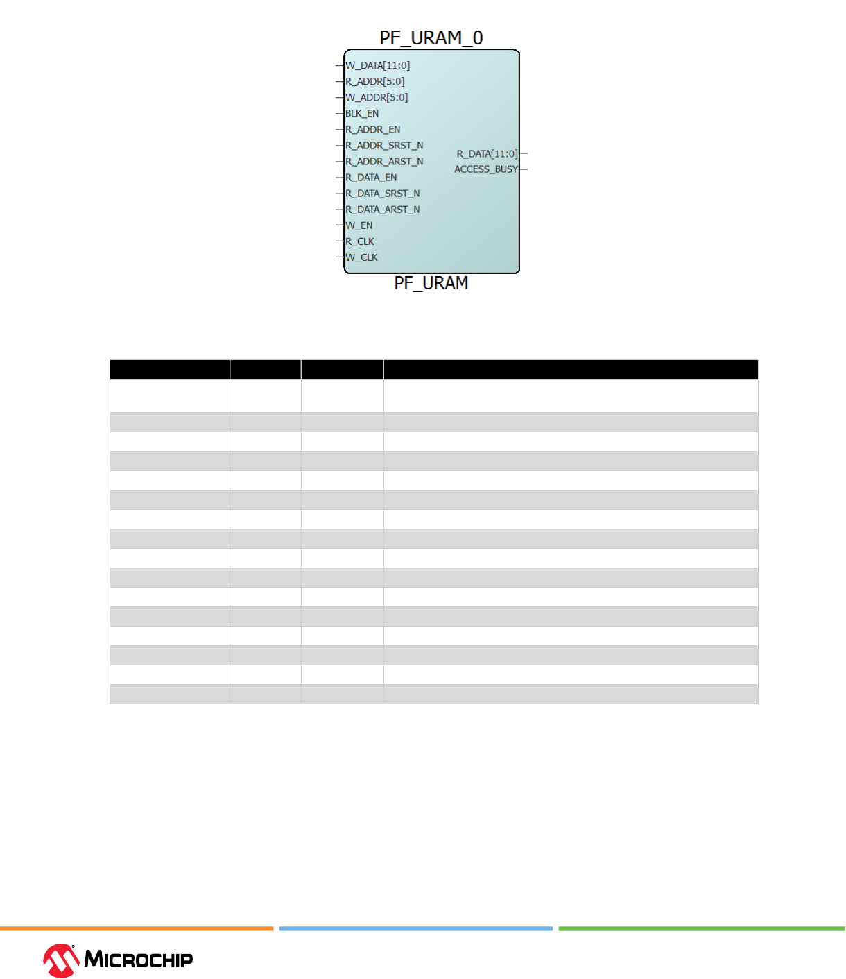
Embedded Memory Blocks
User Guide
© 2023 Microchip Technology Inc. and its subsidiaries
DS60001725G - 41
Figure 2-24. µSRAM Congurator: Generated Component
Table 2-12. μSRAM Congurator Signals
Port Direction Polarity Description
CLK Input Rising edge Single clock signal that drives both ports with the same clock.
Applicable only when Single clock is selected.
BLK_EN Input Active high Read port enable
R_ADDR[5:0] Input — Read address
R_ADDR_EN Input Active high Read address register enable
R_ADDR_SRST_N Input Active low Read address register synchronous reset
R_ADDR_ARST_N Input Active low Read address register asynchronous reset
R_CLK Input Rising edge Read clock. Applicable only when independent clocks are selected.
R_DATA[11:0] Output — Read data
R_DATA_EN Input Active high Read data register enable
R_DATA_SRST_N Input Active low Read data register synchronous reset
R_DATA_ARST_N Input Active low Read data register asynchronous reset
W_ADDR[5:0] Input — Write address
W_CLK Input Rising edge Write clock. Applicable only when independent clocks are selected.
W_EN Input Active low Write enable
W_DATA[11:0] Input — Write data
ACCESS_BUSY Output Active high Busy signal from SmartDebug
This section also describes the μSRAM conguration and denes how the signals are connected.
The μSRAM congurator window has three tabs for settings:
• Parameter settings
• Port settings
• Memory Initialization settings
2.2.4.2.1 Parameter Sengs (Ask a Queson)
The parameter settings include the optimization of μSRAM for High Speed or Low Power, clock signal
settings, and optional port settings.
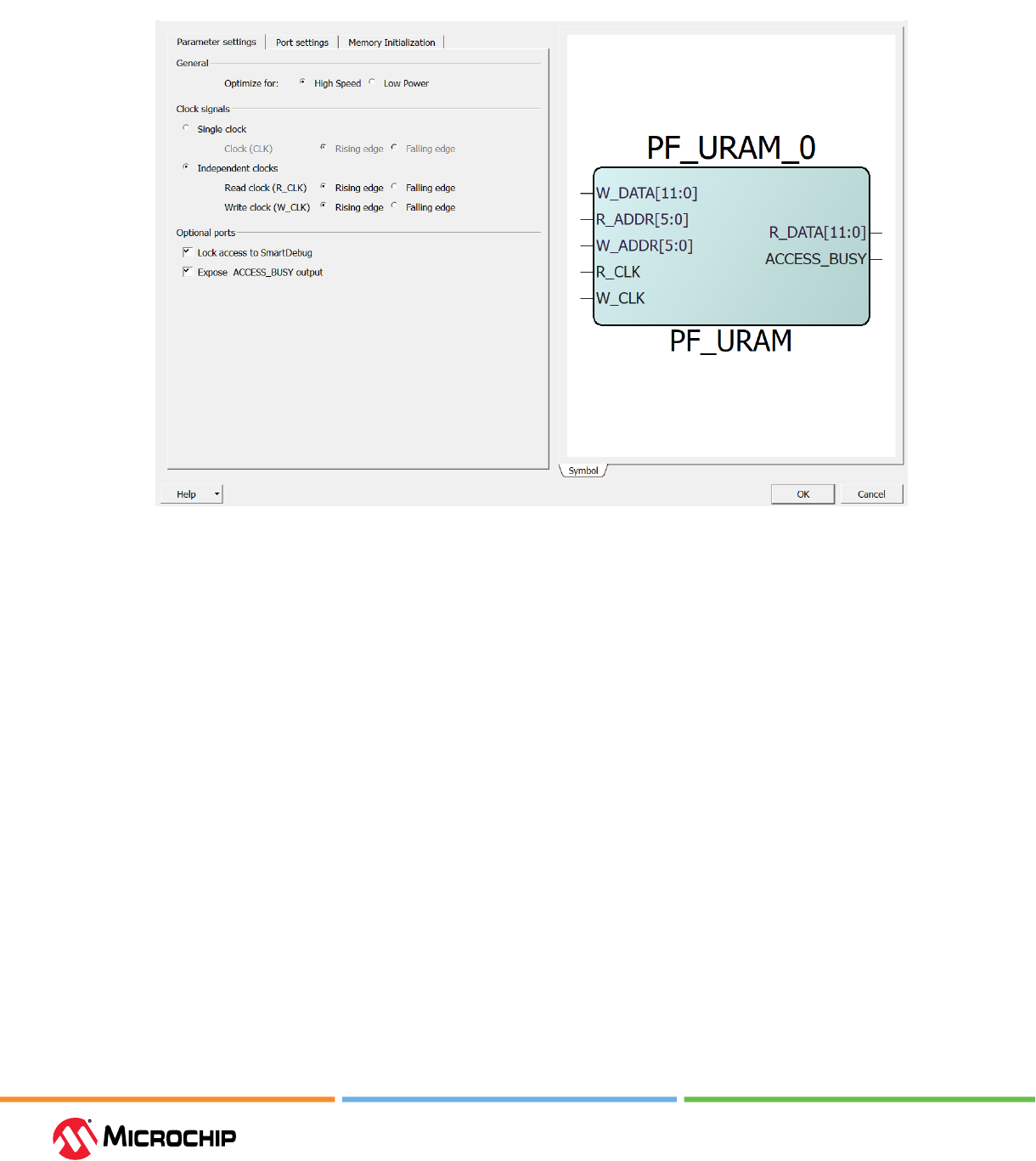
Embedded Memory Blocks
User Guide
© 2023 Microchip Technology Inc. and its subsidiaries
DS60001725G - 42
The following gure shows the μSRAM congurator.
Figure 2-25. MicroSRAM Congurator: Parameter Sengs
Optimization for High Speed or Low Power
The user can optimize the μSRAM macro with one of the following options:
• High Speed—to optimizes the μSRAM macro for speed and area by using width cascading.
• Low Power—to optimizes the μSRAM macro for low power, but it also uses additional logic at the
input and output by using depth cascading.
Single Clock (CLK) or Independent Clocks (R_CLK and W_CLK)
The user can set the clock signals and the signal polarity as follows:
• Single clock—drives both write and read ports with the same clock. This is the default
conguration for μSRAM.
• Independent clocks—selects the independent clock for each port (R_CLK for read port and
W_CLK for write port).
• Rising edge or Falling edge—changes the signal polarity.
Optional Ports
The user can select one of the following optional ports:
• Lock access to SmartDebug—when enabled, SmartDebug access to the RAM is disabled.
• Expose ACCESS_BUSY output—when enabled, SmartDebug ACCESS_BUSY signal is available as
top-level port.
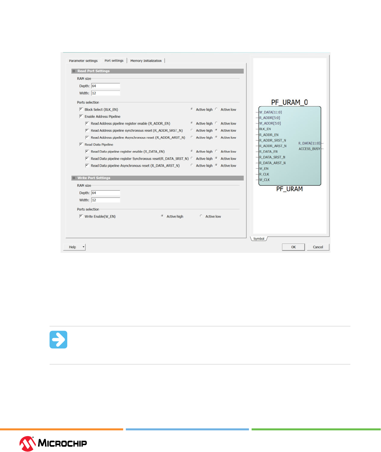
Embedded Memory Blocks
User Guide
© 2023 Microchip Technology Inc. and its subsidiaries
DS60001725G - 43
2.2.4.2.2 Port Sengs (Ask a Queson)
In the Port settings tab, you can set RAM size, select ports, and set data output on write settings for
both write and read ports. The following gure shows the μSRAM IP block port settings.
Figure 2-26. MicroSRAM Congurator: Port Sengs
RAM Size
The user can set the RAM size using the following options.
• Depth—sets the depth range. The depth range for each port is 1 to 2048. The maximum value
depends on the die.
• Width—sets the width range. The width range for each port is 1 to 53280.
Important: The two ports can be congured independently for any depth and width. Write
depth x write width must be equal to read depth x read width. The width and depth range
varies for dierent devices. The performance of the RAM is aected if width and depth are
too large.
Port Selection: Block Select for Read Port (BLK_EN)
The default conguration for BLK_EN is unchecked, which ties the signal to the Active state and
removes it from the generated macro. For more information, see 2.2.1. Read Operation. Select
Active high or Active low to change the signal polarity.

Embedded Memory Blocks
User Guide
© 2023 Microchip Technology Inc. and its subsidiaries
DS60001725G - 44
Important: Ports are populated on the component by checking its respective check-boxes.
Write Enable (W_EN)
The default conguration for W_EN is unchecked (disabled), which ties the signal to the Active state
and removes it from the generated macro. For more information, see 2.2.2. Write Operation. Select
Active high or Active low to change the signal polarity.
Important: You can insert the signal on the generated macro by checking the respective
check-boxes.
Enable Address Pipeline
Check the Enable Address Pipeline check box to enable pipelining of Read data (R_ADDR_EN). This
is a static selection and cannot be changed dynamically by driving it with a signal. If the Enable
Address Pipeline check box is not checked, the user cannot congure R_ADDR_EN,R_ ADDR_SRST_N,
or R_ADDR_ARST_N signals.
• Register Enable (R_ADDR_EN and R_DATA_EN): the pipeline registers for read ports have Active
high enable inputs. By default, the check box is disabled. Selecting this check box adds the signal
to the top-level port.
• Synchronous Reset (R_ADDR_SRST_N and R_DATA_SRST_N): the pipeline registers for read ports
have Active low, synchronous reset inputs. By default, the check box is disabled. Selecting this
check box adds the signal to the top-level port.
• Asynchronous Reset (R_ADDR_ARST_N and R_DATA_ARST_N): the pipeline registers for read
ports have Active low, asynchronous reset inputs. By default, the check box is disabled. Selecting
this check box adds the signal to the top-level port.
• Active high or Active low: changes the signal polarity.
Important: Ports are populated on the component by checking the respective check
boxes.
Read Data Pipeline—This option is disabled by default. Select the Pipeline check box to enable
pipelining of Read data (R_DATA). This is a static selection and cannot be changed dynamically by
driving it with a signal. Turning o pipelining of Read data also disables the conguration options of
the respective R_DATA_EN, R_DATA_SRST_N, and R_DATA_ARST_N signals.
2.2.4.2.3 Memory Inializaon at Power-Up (Ask a Queson)
In the Memory Initialization tab, the user can initialize RAM at power-up. μSRAM can be initialized
during device power-up and functional simulation as described in Memory Initialization at Power-
Up of 2.1.3.2.1. Dual-Port Large SRAM Congurator. The following gure shows the μSRAM IP
memory initialization.
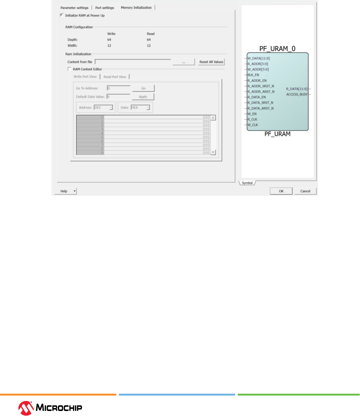
Embedded Memory Blocks
User Guide
© 2023 Microchip Technology Inc. and its subsidiaries
DS60001725G - 45
Figure 2-27. MicroSRAM Congurator: Memory Inializaon
The Reset All Values option resets all the data values. This option is enabled when the RAM
Content Editor check box is selected.
2.2.4.3 μSRAM Memory Macro (Ask a Queson)
A μSRAM primitive is available as a component that can be used directly in the HDL le or
instantiated in SmartDesign. For more information about conguring μSRAM, see 5.2. μSRAM
Macro.
2.3 μPROM (Ask a Queson)
Both device families include a single User Programmable Read-Only Memory (μPROM) row located
at the bottom of the fabric, providing up to 513 KB of non-volatile, read-only memory. The address
bus is 16 bits wide, and the read data bus is 9-bit wide. Fabric logic has read-only access to the entire
μPROM data. The following gure shows the high-level block diagram of μPROM.
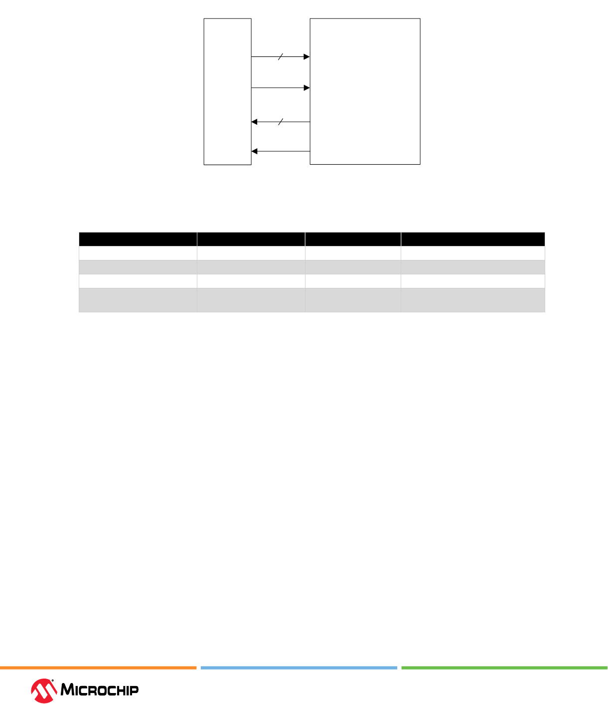
Embedded Memory Blocks
User Guide
© 2023 Microchip Technology Inc. and its subsidiaries
DS60001725G - 46
Figure 2-28. Simplied Funconal Block Diagram of μPROM
µPROM
Fabric
Logic
ADDR[15:0]
BLK
DATAR[8:0]
BUSY
The following table lists the ports of μPROM.
Table 2-13. μPROM Port List
Port Name Direction Polarity Description
ADDR[15:0] Input — Address input
BLK Input Active-High Block select
DATAR[8:0] Output — Read data output
BUSY Output Active-High Asserted when system controller or
SmartDebug is accessing the µPROM
2.3.1 μPROM Architecture and Address Space (Ask a Queson)
Architecturally, the μPROM is structured into dierent memory arrays with 8-bit addressing. Each
array is 256 x 9 bit words. The total number of memory array per device is die-dependent and can
vary from 194 for the smallest die (MPFS025) to 553 for the largest die (MPFS460). The address bus
(ADDR) is 16 bits wide. The lower 8 bits, ADDR [7:0], are used to address the individual 9-bit words
while the upper 8 bits, ADDR[15:8], are used to address the individual memory array blocks inside
the device.
The following gure shows a simplied block diagram of the μPROM memory.
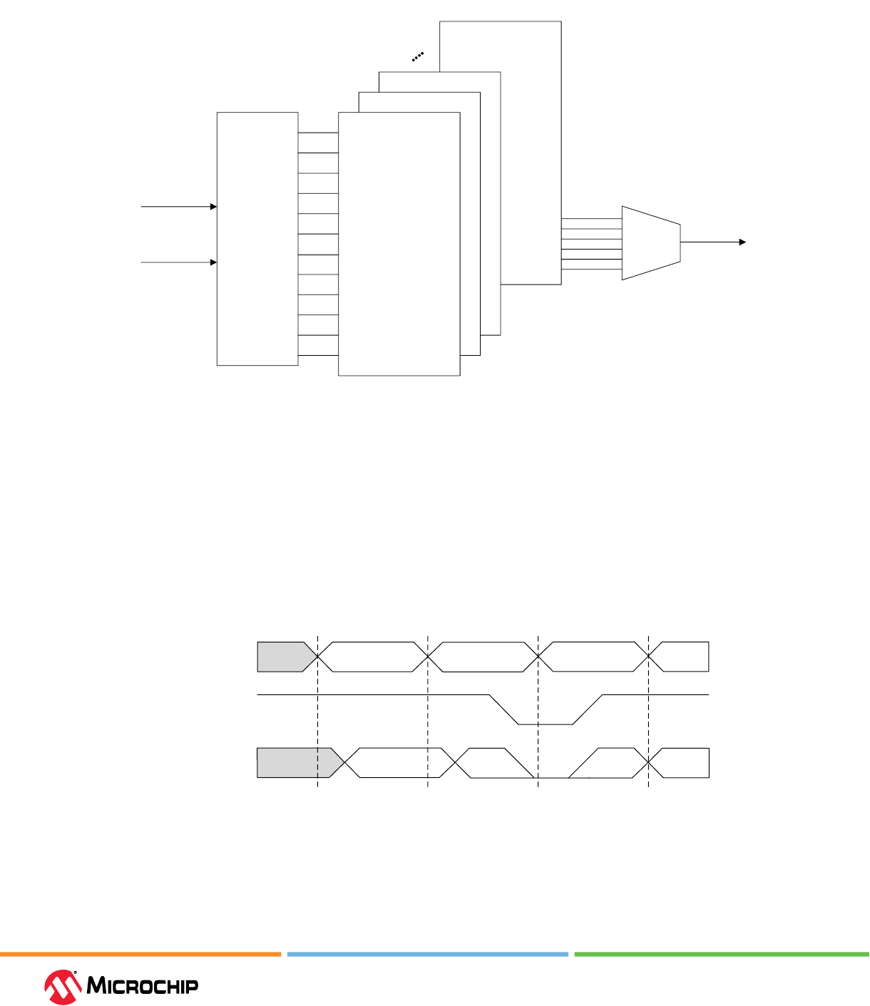
Embedded Memory Blocks
User Guide
© 2023 Microchip Technology Inc. and its subsidiaries
DS60001725G - 47
Figure 2-29. µPROM Memory Blocks
ADDR[15:0]
BLK
µPROM
Interface
256 × 9
Memory
Array
Read
Decoder
DATAR[8:0]
256 × 9
Memory
Array
2.3.2 μPROM Operaon (Ask a Queson)
In μPROM, the write operation (program/erase) is performed during FPGA Programming. To
congure the μPROM, the Libero SoC μPROM congurator writes the memory le (*.mem) to the
conguration bit-stream. The memory le is a plain text le. The device programmer (FlashPro 5 or
later) writes this memory le to μPROM during FPGA programming. Read operations are performed
only through the fabric interface. All μPROM read operations are asynchronous. To perform a
synchronous read operation, the μPROM output needs to be pipelined using fabric registers.
The following gure shows the read timing diagram for the μPROM.
Figure 2-30. Read Operaon in µPROM
ADDR[15:0]
BLK
DATAR[8:0]
A0
A1
A2
D(A1)
D(A2)
A3
D(A0)
D(A3)
2.3.3 Implementaon (Ask a Queson)
The μPROM can be implemented using the Congurator available in the Catalog tab. To invoke the
congurator:
1. Expand Memory & Controllers in the Catalog.

Embedded Memory Blocks
User Guide
© 2023 Microchip Technology Inc. and its subsidiaries
DS60001725G - 48
2. Do one of the following to invoke the μPROM Congurator:
– Double click or right click PF μPROM and select Instantiate in design_name to instantiate
the μPROM in the SmartDesign canvas.
– Double click or right click PF μPROM and select Congure Core. Enter a component name
for the μPROM when prompted.
Figure 2-31. µPROM Core in Catalog
3. In the μPROM Congurator, click Add Clients to System to add a client to the μPROM. The
following gure shows the μPROM Congurator. Only the client is programmed and not all the
content is erased during programming.
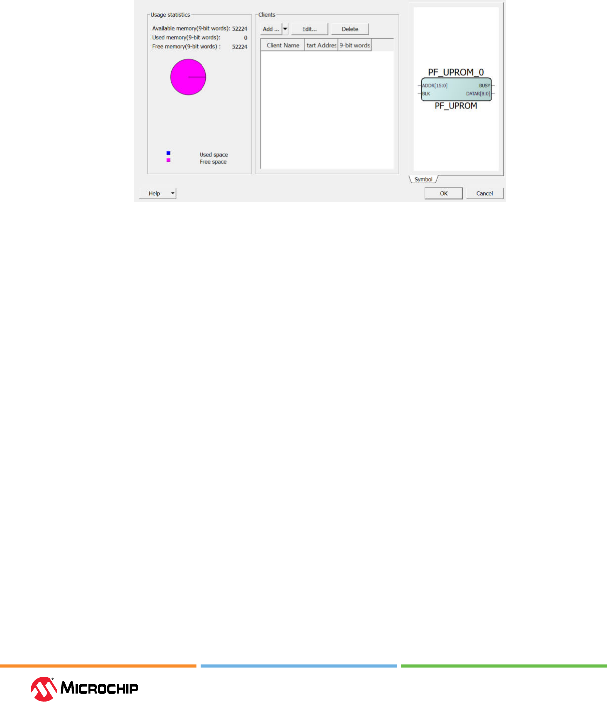
Embedded Memory Blocks
User Guide
© 2023 Microchip Technology Inc. and its subsidiaries
DS60001725G - 49
Figure 2-32. µPROM Congurator
2.3.3.1 Usage Stascs (Ask a Queson)
Usage statistics display the total memory size of the μPROM, the size of used memory, and available
free memory. All memory sizes are expressed in terms of the number of 9-bit words.
2.3.3.1.1 Available Memory (Ask a Queson)
The μPROM can hold upto 58,368 9-bit words (total 525312 bits), depends on the die. For more
information, see Table 2.
2.3.3.1.2 Used Memory (Ask a Queson)
When memory clients are added, the used memory displays the total amount of memory (number
of 9-bit words) used by all clients. This is displayed in blue in the pie chart.
2.3.3.1.3 Free Memory (Ask a Queson)
Free memory (number of 9-bit words) is displayed in magenta in the pie chart.
2.3.3.2 Add Clients to System (Ask a Queson)
1. Click Add Clients to System to open the Add Data Storage Client dialog box (Figure 2-33).
2. Specify the start address, client size, the content of the client, and whether to use the memory
content for simulation or not.
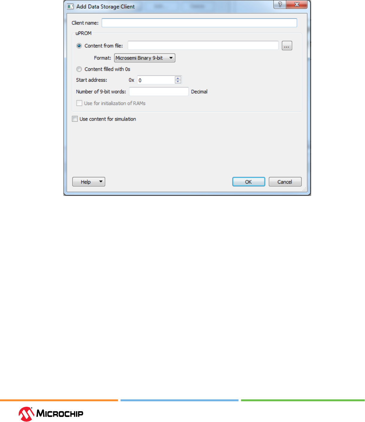
Embedded Memory Blocks
User Guide
© 2023 Microchip Technology Inc. and its subsidiaries
DS60001725G - 50
Figure 2-33. Add Data Storage Client Dialog Box
2.3.3.2.1 Client Name (Ask a Queson)
Enter a name for your memory client.
2.3.3.2.2 Content from File (Ask a Queson)
Import the memory client from a memory le with this option. Click Browse to navigate to the
location of the memory le and import. Select the Memory File and click Open.
Note: In this example, *.mem le is selected.
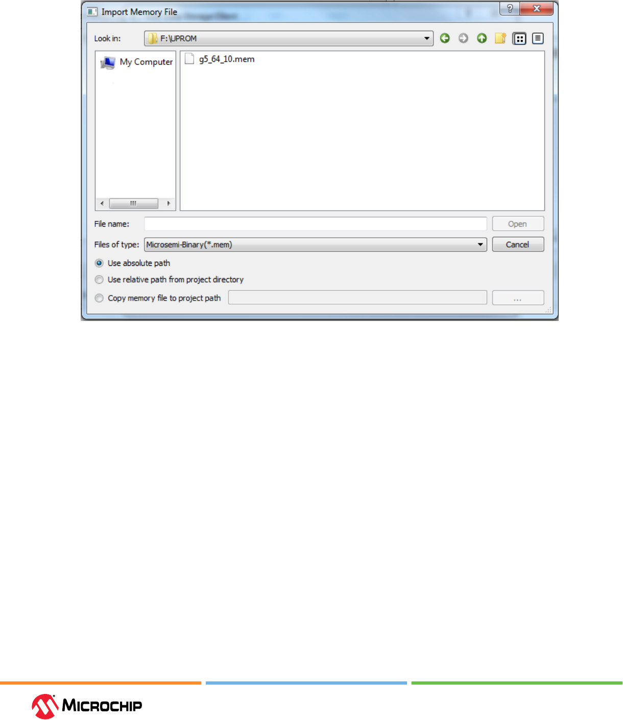
Embedded Memory Blocks
User Guide
© 2023 Microchip Technology Inc. and its subsidiaries
DS60001725G - 51
Figure 2-34. Import Memory File Dialog Box
Use Absolute Path
When this is selected, the absolute path of the memory le appears in the Content from File eld.
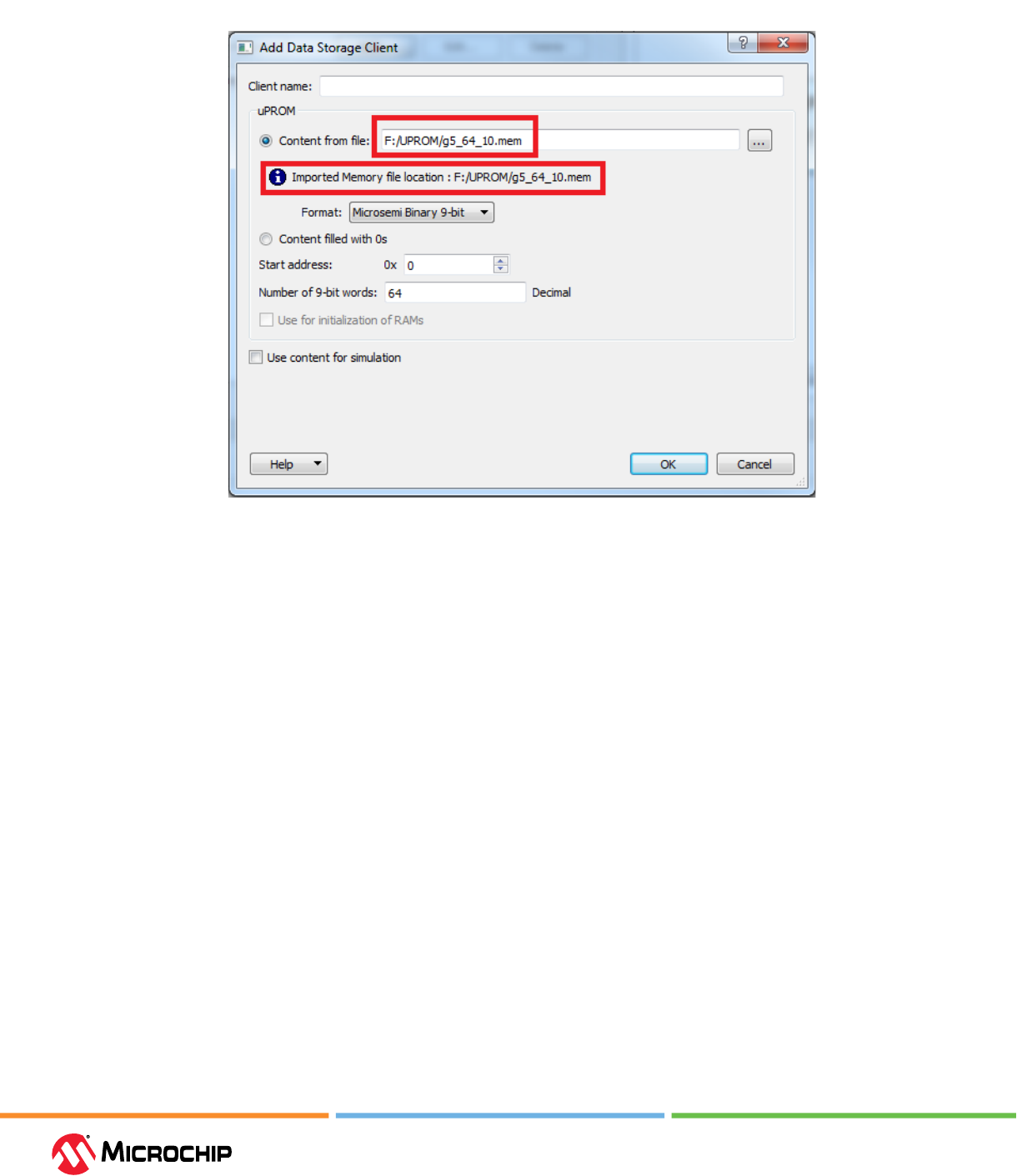
Embedded Memory Blocks
User Guide
© 2023 Microchip Technology Inc. and its subsidiaries
DS60001725G - 52
Figure 2-35. Absolute Path of Memory File
Use Relative Path from Project Directory
When this is selected, the Relative Path of the Memory File (relative to the Project location) is
displayed in the Content from File eld.
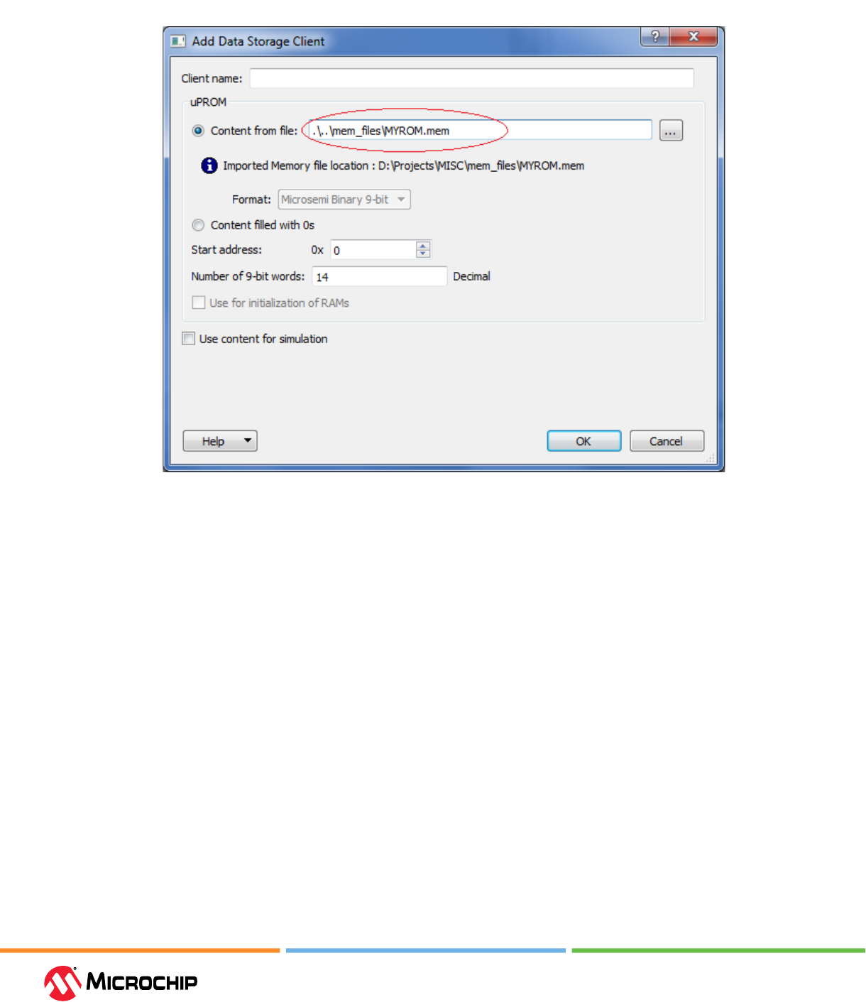
Embedded Memory Blocks
User Guide
© 2023 Microchip Technology Inc. and its subsidiaries
DS60001725G - 53
Figure 2-36. Relave Path of Memory File
Copy Memory File to Project Path
Select this option and click Browse to navigate to the location of the memory le to copy from. The
memory le is copied to the project location.
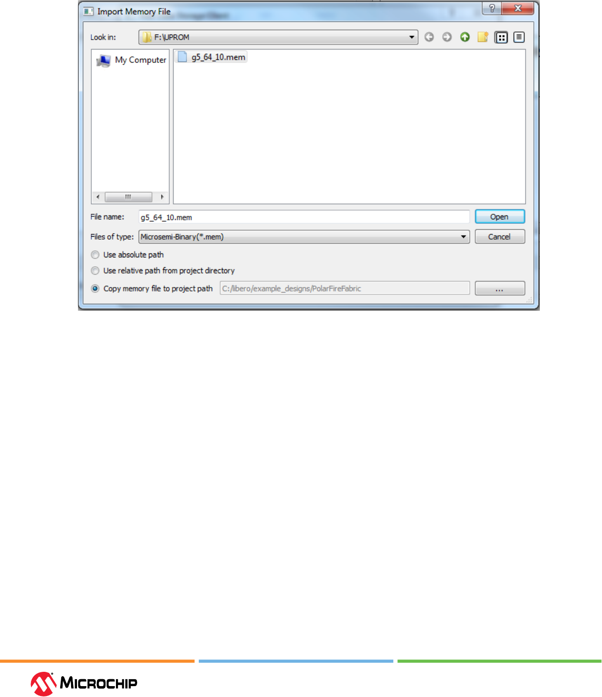
Embedded Memory Blocks
User Guide
© 2023 Microchip Technology Inc. and its subsidiaries
DS60001725G - 54
Figure 2-37. Locaon of Memory File to Copy From
Note: On the Windows
®
systems, if the memory le and the Project location are on dierent drives,
the Absolute Path is used even if Relative Path is selected.
The memory le cannot be copied to and stored in the project's subfolders: component,
smartgen, synthesis, designer, simulation, stimulus, tool data, and constraint. To prevent users from
inadvertently copying the memory le into these sub-folders, these project subfolders are hidden
from view when you select the project folder. Copy the memory le to the same project folder as the
*.prjx le.
Note: The copied Memory File path is internally stored as relative path. Once this is copied
to the project, user must update the content of the Memory File to make it current. μPROM
supports Intel-Hex (*.hex, *.ihx), Motorola-S (*.s), Simple-Hex (*.shx), and Microsemi-
Binary (*.mem) memory le formats. For more information about the supported memory le
formats, see 4. Appendix: Supported Memory File Formats for LSRAM and μSRAM.
In this example, *.mem is used. The *.mem le must meet the following requirements:
• Each row is one 9-bit binary word (only 0s and 1s).
• The number of rows in the le (word count) must be less than or equal to the memory space of
the μPROM (up to 58,368 words).
• The memory le must have the *.mem le extension. The following gure shows an example
memory le.
Embedded Memory Blocks
User Guide
© 2023 Microchip Technology Inc. and its subsidiaries
DS60001725G - 55
Figure 2-38. Microsemi Binary File (*.mem) Example
2.3.3.2.3 Content lled with 0s (Ask a Queson)
Fill the content of the memory client with 0s as a place holder and update the memory client after
Place and Route and before Programming. There is no need to rerun Place and Route after updating
the μPROM Memory Content. For more information, see 2.3.3.6. Update μPROM Memory Content.
2.3.3.2.4 Start Address (Ask a Queson)
Enter the Start address (16-bit) of the client in HEX.
2.3.3.2.5 Number of 9-bit Words (Ask a Queson)
Enter the size of the client (displayed as the number of 9-bit words) in decimal.
Note: When multiple clients are added, ensure that the address range of each client does not
overlap with the other clients. Overlapping of address range is not allowed and is agged as an error
when it occurs.
2.3.3.2.6 Use Content for Simulaon (Ask a Queson)
Select to include the memory content for simulation. When this checked, a UPROM.mem le is
automatically created in the <prj_location>/simulation folder when simulation is invoked in
the Design Flow window. The UPROM.mem le is read by the μPROM simulation model to initialize the
μPROM content when the simulation starts. Only clients with the Use Client for Simulation check
box checked have the contents added to the UPROM.mem le for simulation.
The following gure shows the added clients under User clients in μPROM.
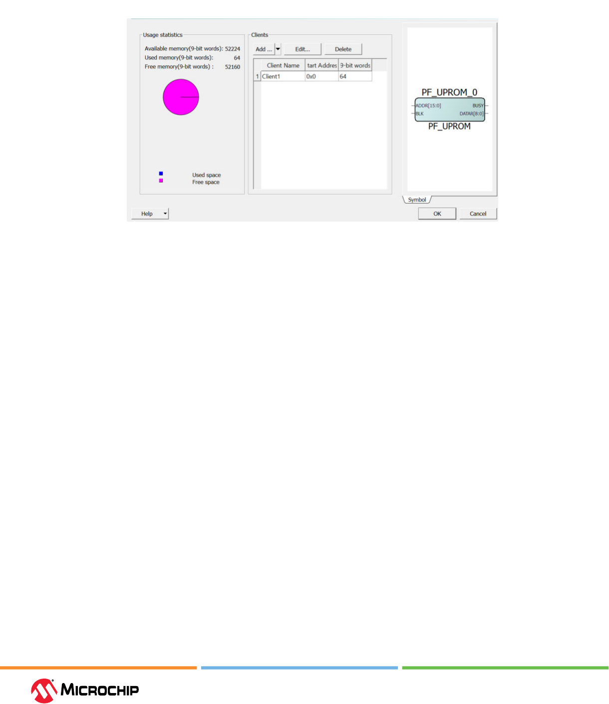
Embedded Memory Blocks
User Guide
© 2023 Microchip Technology Inc. and its subsidiaries
DS60001725G - 56
Figure 2-39. User Clients
2.3.3.3 DRC Rules and Error Messages (Ask a Queson)
To prevent out-of-bound memory addressing and overlapping of address space, DRC rules are
enforced and error messages are given when:
• An invalid start address (outside of the μPROM memory space) is entered.
DRC Error: The specied start address is invalid; legal addresses range from 0x0 to
<max_possible_address_for_the_die>.
• The start address and the number of words entered put the user client beyond the memory
space of the μPROM.
DRC Error: For the specied start address, the number of words cannot exceed the total number
of words of <max_possible_words_for_die>.
• The number of 9-bit words entered is less than the number of words in the memory le used to
ll the content of the client.
DRC Error: The number of words cannot be less than the number of words
<mem_le_word_count> specied in the memory le <mem_le_name>.
• There is more than one user client and the address range of one client overlaps with that of
another.
DRC Error: This client overlaps with: <client name >.
• The memory le (*.mem) size exceeds the total μPROM memory space.
DRC Error: The memory le <memoryFileName> size exceeds the total μPROM space.
2.3.3.4 Eding a Client (Ask a Queson)
To edit a client:
1. Click Edit or right-click the client name and select Edit to open the Edit Data Storage Client
dialog box.
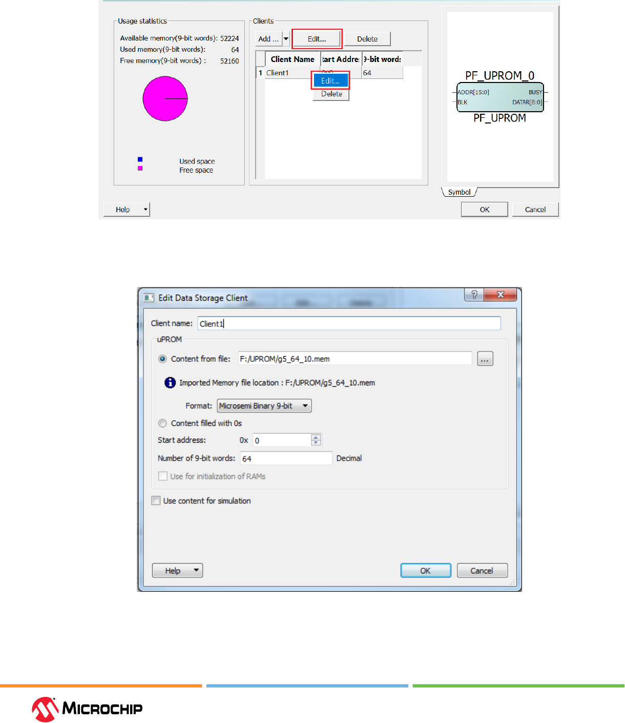
Embedded Memory Blocks
User Guide
© 2023 Microchip Technology Inc. and its subsidiaries
DS60001725G - 57
Figure 2-40. Eding User Clients
2. Make changes in the Edit Data Storage Client dialog box and click OK to save edits.
Figure 2-41. Edit Data Storage Client Dialog Box
2.3.3.5 Deleng a Client (Ask a Queson)
Right-click the client and select Delete.
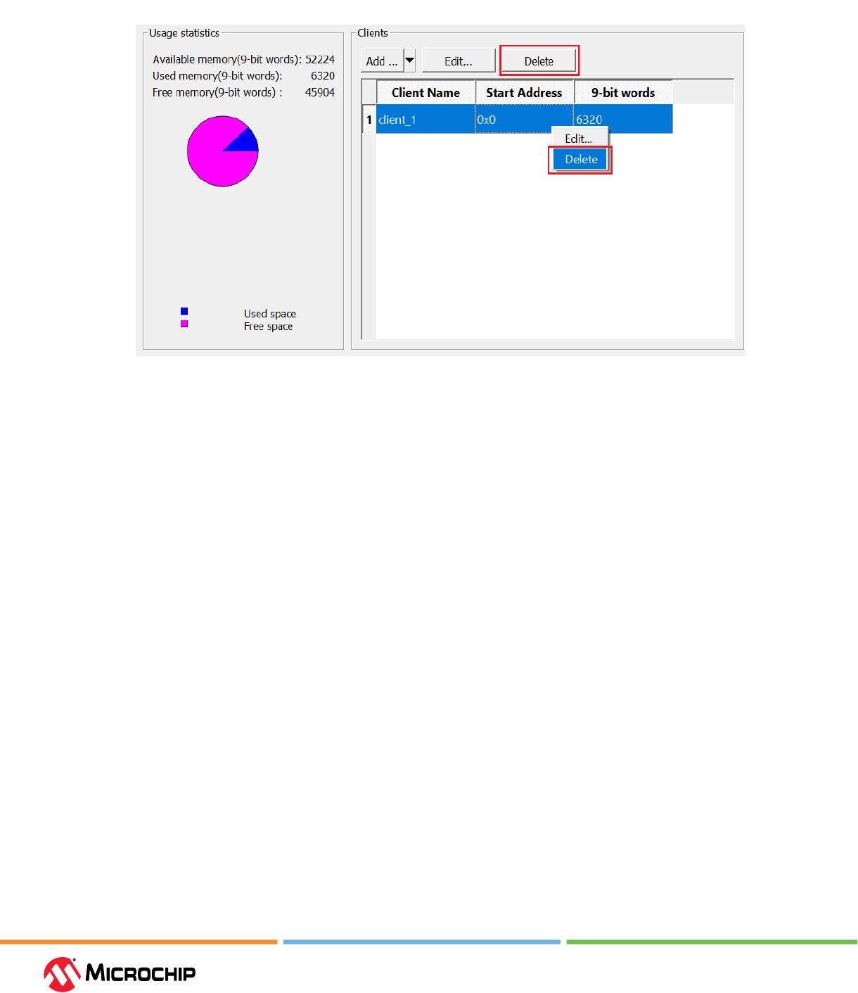
Embedded Memory Blocks
User Guide
© 2023 Microchip Technology Inc. and its subsidiaries
DS60001725G - 58
Figure 2-42. Deleng a Client
2.3.3.6 Update μPROM Memory Content (Ask a Queson)
The μPROM Memory Content can be updated after Place and Route using Device Conguration
and Memory Initialization under Program and Debug Design in the Design Flow tab. For more
information about updating μPROM memory content, see PolarFire Family Power-Up and Resets
User Guide.
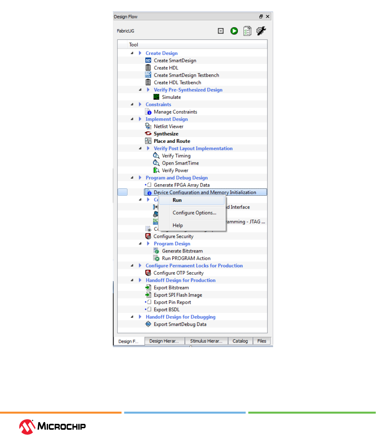
Embedded Memory Blocks
User Guide
© 2023 Microchip Technology Inc. and its subsidiaries
DS60001725G - 59
Figure 2-43. Update µPROM Memory Content
2.4 sNVM (Ask a Queson)
The PolarFire family includes 56 KB of sNVM. The sNVM is organized into 221 pages of 236 bytes or
252 bytes depending on whether the data is stored as plain text or encrypted/authenticated data.
Embedded Memory Blocks
User Guide
© 2023 Microchip Technology Inc. and its subsidiaries
DS60001725G - 60
Pages within the sNVM can be marked as ROM during bitstream programming. Data written to the
sNVM can be protected by the Physically Unclonable Function (PUF). The sNVM is readable and
writable by the designer’s application during runtime and is an ideal storage location for locating the
boot code for soft processors and user keys.
2.4.1 Implementaon (Ask a Queson)
The sNVM is not accessible to the fabric logic. You can access sNVM through CoreSysService IP using
system service calls. The sNVM content is used for device initialization for LSRAM, μSRAM, PCIe,
and transceiver data. Few pages of available 56 KB are used for storing the device and peripheral
conguration data and the remaining pages store the user data. For more information about device
initialization using sNVM, see PolarFire Family Power-Up and Resets User Guide.
4136 bytes of sNVM storage space is required to initialize a single LSRAM block (1024 x 20 bits) with
custom data or all zeros. 168 bytes of sNVM storage space is required to initialize a single Micro
SRAM block (64 x 12 bits) with custom data or all zeros. Each page of sNVM can store 252 bytes. So,
to store 168 bytes of a single μSRAM block, you need one sNVM page.
The selected logical width/depth determines the number of LSRAM or Micro SRAM blocks
instantiated. Therefore, the number of fabric RAM blocks, the user chooses to initialize during
Power-Up, determines how much non-volatile storage space (such as sNVM) is required for the
system controller operation, and how long the device initialization process takes to complete. To
obtain a design specic summary of the sNVM usage and Power-Up to Functional Time (PUFT),
the user must run the Libero SoC Design Flow Production Hando step called Export Design
Initialization Data and Memory Report, as shown in the following gure.
Figure 2-44. Export Design Inializaon Data and Memory Report
2.5 eNVM (PolarFire SoC Only) (Ask a Queson)
PolarFire SoC devices include 128 Kbytes of eNVM within the MSS. eNVM is used for storing the
rst stage boootloader during the device programming. At device power-up, the E51 monitor core
boots from the eNVM and holds the U54 processors in reset. The E51 core boots the U54 cores
based on the boot addresses specied in the rst stage bootloader. For more information about
device initialization using eNVM, see PolarFire Family Power-Up and Resets User Guide. For more
information about booting and conguration, see PolarFire SoC Software Development and Tool
Flow User Guide.

Math Blocks
User Guide
© 2023 Microchip Technology Inc. and its subsidiaries
DS60001725G - 61
3. Math Blocks (Ask a Queson)
In the PolarFire family, fabric includes embedded Math blocks optimized for Digital Signal Processing
(DSP) applications such as Finite Impulse Response (FIR) lters, Innite Impulse Response (IIR) lters,
Fast Fourier Transform (FFT) functions, and encoders that require high data throughput.
Math block has a built-in multiplier, a pre-adder, and an adder. These built-in features minimize the
external logic required to implement multiplication, multiply-add, and Multiply-Accumulate (MACC)
functions. For more information about Math block inference by Synplify Pro ME, see Inferring
PolarFire MACC Blocks Application Note. Implementation of these arithmetic functions using math
blocks results in ecient resource usage and improved performance for DSP applications. Math
blocks can also be used in conjunction with fabric logic and embedded memories (LSRAM, μSRAM,
and μPROM) to implement complex DSP algorithms.
3.1 Features (Ask a Queson)
Key features of the Math block are as follows:
• High-performance and power optimized multiplication operations.
• Full-precision 48-bit output width.
• Supports 18 x 19 signed multiplication.
• Supports 17 x 18 unsigned multiplications.
• Supports input and output pipeline registers.
• Supports Dot-Product (DOTP) mode.
• Supports Single-Instruction Multiple-Data (SIMD) mode (Dual-Independent mode).
• Internal pre-adder block enables the ecient implementation of symmetric lters.
• Supports input cascade chain to form the tap-delay line for ltering applications.
• Built-in addition, subtraction, and accumulation units to combine multiplication results eciently.
• Independent 48-bit registered third input.
• Supports signed and unsigned operations.
• Internal cascade signals (48-bit CDIN and CDOUT) enable cascading of the Math blocks.
3.2 Math Block Resources (Ask a Queson)
Table 2 and Table 3 lists the number of Math blocks available in both the device families.
3.3 Funconal Descripon (Ask a Queson)
Math blocks are arranged in rows in the FPGA fabric and can be cascaded in a chain, starting from
the left-most block to the right-most block within a row.
Each Math block consists of:
• 3.3.1. Pre-Adder
• 3.3.2. Multiplier
• 3.3.3. Adder/Subtractor
• 3.3.4. Math Block Ports
• 3.3.5. 16 x 18 Coecient ROM and B2 Register
The following gure shows the simplied block diagram of the Math block.
Math Blocks
User Guide
© 2023 Microchip Technology Inc. and its subsidiaries
DS60001725G - 62
Figure 3-1. Simplied Funconal Block Diagram of Math Block
SUB
37
48
A[17:0]
C[47:0]
B[17:0]
ARSHFT17
CDIN_FDBK_SEL[1:0]
0
ROM_ADDR[3:0]
D[17:0]
16 × 18
ROM*
BCIN[17:0]
BCOUT[17:0]
PASUB
CARRYIN
Multiplier
Pre-adder
00
11
01
>> 17
48
19
18
Note: *B2 register, 16 × 18 coefficient ROM, and outside MUXes use the Interface Logic in the fabric.
E
CLK
CDIN[47:0]
SUB
Reg
A Reg
B Reg
D Reg
PASUB
Reg
C Reg
SHFT
Reg
SEL
Reg
B2
Reg*
+/-
OVFL_CARRYOUT
P[47:0]
CDOUT[47:0]
Output
Registers
Adder/Subtractor
+/-
The following table lists the ports of the Math block.
Table 3-1. Port List for Math Block
Port Name Direction Type Polarity Description
A[17:0] Input Dynamic Active high Input data for operand A when USE_ROM = 0
ARSHFT17 Input Dynamic Active high Arithmetic right-shift for operand E.
When asserted, a 17-bit arithmetic right-shift is
performed on operand E
B[17:0] Input Dynamic Active high Input data B to pre-adder with data D
B2[17:0] Output Dynamic Active high Pipelined output of input data B. Result P must be
oating when B2 is used.
BCOUT[17:0] Output Cascade Active high Cascade output of B2. Value of BCOUT is the same
as B2. The entire bus must either be dangling or
drive an entire B input of another MACC_PA or
MACC_PA_BC_ROM block.
C[47:0] Input Dynamic Active high Input data C
When DOTP = 1, connect C[8:0] to CARRYIN.
When SIMD = 1, connect C[8:0] to 0.
CLK Input Dynamic Rising edge Clock for A, B, C, CARRYIN, D, P, OVFL_CARRYOUT,
ARSHFT17, CDIN_FDBK_SEL, PASUB, and SUB registers
CARRYIN Input Dynamic Active high CARRYIN for input data C
CDIN[47:0] Input Cascade Active high Cascaded input for operand E
The entire bus must be driven by an entire CDOUT of
another Math block. In Dot-product mode, the driving
CDOUT must also be generated by a Math block in
Dot-product mode.
Math Blocks
User Guide
© 2023 Microchip Technology Inc. and its subsidiaries
DS60001725G - 63
...........continued
Port Name Direction Type Polarity Description
CDIN_FDBK_SEL[1:0] Input Dynamic Active high Select CDIN, P, or 0 for operand E
CDOUT[47:0] Output Cascade Active high Cascade output of result P
Value of CDOUT is the same as P. The entire bus must
either be dangling or drive an entire CDIN of another
Math block in cascaded mode.
D[17:0] Input Dynamic Active high Input data D to pre-adder with data B
When SIMD = 1, connect D[8:0] to 0.
OVFL_CARRYOUT Output — Active high OVERFLOW or CARRYOUT
P[47:0] Output — Active high Result data
PASUB Input Dynamic Active high Subtract operation for pre-adder of B and D
ROM_ADDR[3:0] Input Dynamic Active high Address of ROM data for operand A when USE_ROM =
1
SUB Input Dynamic Active high Subtract operation
Note: For information about asynchronous reset, synchronous reset, bypass, and enable signal
details for each input/output register, see Table 5-17.
3.3.1 Pre-Adder (Ask a Queson)
Pre-adder performs the upstream addition/subtraction operation prior to multiplication. It is
congured for the following operations on the inputs B[17:0] and D[17:0]:
• 18-bit addition/subtraction, producing the result B[17:0] ± D[17:0]. For more information, see
Figure 3-6.
• Two 9-bit additions/subtractions, producing the results B[8:0] ± D[8:0], B[17:9] ± D[17:9]. For
more information, see Figure 3-7. In the two 9-bit adder/subtractor modes, the type of operation
(addition/subtraction) performed on the lower pre-adder of bits B[8:0] and D[8:0], and the type of
operation performed on the upper pre-adder of bits B[17:9], D[17:9] must be the same.
• Single 9-bit addition/subtraction, producing the result B[17:9] ± D[17:9]. For more information,
see Figure 3-8.
3.3.2 Mulplier (Ask a Queson)
Inputs to multiplier are Port A data and pre-adder output data. The Math block multiplier can be
congured to perform any of the following:
• 19 x 18-bit multiplication.
• Two 10 x 9-bit multiplications (dot-product).
• Two independent multiplications, one 9 x 9-bit and one 10 x 9-bit SIMD/(dual-independent
mode).
3.3.3 Adder/Subtractor (Ask a Queson)
The adder/subtractor performs the nal addition/subtraction and accumulation operation. This
operation produces the nal Math block output with 48-bit precision.
The adder/subtractor can be congured to compute any of the following:
• (B ± D) x A + C + CARRYIN or (B ± D) x A + E.
• (B ± D) x A + C + CARRYIN + E.
If this block is congured as a subtractor, the output is (C + E) - (B ± D) x A.
3.3.4 Math Block Ports (Ask a Queson)
Math blocks have built-in, by-passable registers on the data inputs (A, B, C, and D), data output (P),
and control signals.

Math Blocks
User Guide
© 2023 Microchip Technology Inc. and its subsidiaries
DS60001725G - 64
3.3.4.1 C Input and CARRYIN (Ask a Queson)
The C input port allows the formation of several 3-input mathematical functions, such as 3-input
addition or 2-input multiplication with addition. The CARRYIN signal is the carry input of the
adder or accumulator. The C input can also be used as a dynamic input to achieve the following
functionalities:
• Wrapping-around the cascade chain of Math blocks from one row to the next row through the
fabric.
• Rounding the multiplication outputs.
• Trimming the lower-order bits of the nal sum, partial sum, or the product.
3.3.4.2 CDIN, CDOUT, and CDIN_FDBK_SEL (Ask a Queson)
Higher-level DSP functions are supported by cascading individual Math blocks in a row. The two
data signals, CDIN[47:0] and CDOUT[47:0], provide the cascading capability with an input select
(CDIN_FDBK_SEL). Table 3-3 lists the possible settings of CDIN_FDBK_SEL for propagating CDIN to the
E input of the adder.
To cascade Math blocks, the CDOUT of one block must feed the CDIN of an adjacent block. The
CDOUT-to-CDIN connection is hardwired between the blocks within a row. Two dierent rows can
be cascaded using fabric routing between two rows. Extra pipeline registers might be required to
compensate for the extra delays added due to the fabric routing, which increases the latency of the
chain.
The ability to cascade Math blocks is useful in lter designs. For example, an FIR lter can be
constructed by cascading inputs to arrange a series of input data samples and cascading outputs
to arrange a series of partial output results. Since the general routing in the fabric is not used,
the cascading ability provides a high-performance and low-power implementation of DSP lter
functions. For more information, see 3.4. Cascading Math Blocks.
3.3.4.3 BCOUT (Ask a Queson)
BCOUT signal forms a chain in a row of Math blocks for the B input. This signal can be used to form
the input delay chain used in lter applications. The BCOUT signal is not hardwired and is routed
using fabric routing.
3.3.4.4 OVFL_CARRYOUT (Ask a Queson)
Each Math block has an overow signal, OVFL_CARRYOUT. This signal indicates any overow from
the addition operation performed by the adder. This signal is also used to extend the adder data
widths from the existing 48 bits using fabric resources. It is also used to implement saturation
capabilities. Saturation refers to catching an overow condition and replacing the output with either
the maximum (most positive) or minimum (most negative) value that can be represented.
Table 3-2. Truth Table for Computaon of OVFL_CARRYOUT
OVFL_CARRYOUT_SEL OVFL_CARRYOUT Description
0 (SUM[49] XOR SUM[48]) OR
(SUM[48] XOR SUM[47])
True, if overow or underow occurred.
1 C[47] XOR E[47] XOR SUM[48] A signal that can be used to extend the
nal adder in the fabric.
3.3.4.5 ARSHFT17 (Ask a Queson)
For multi-precision arithmetic, Math blocks provide a right shift by 17 that is controlled by the shift
input, ARSHFT17. Therefore, a partial product from one Math block can be shifted to the right and
added to the next partial product computed in an adjacent Math block. Using this technique, Math
blocks can be used to build wide multipliers.
Math Blocks
User Guide
© 2023 Microchip Technology Inc. and its subsidiaries
DS60001725G - 65
3.3.4.6 CDIN_FDBK_SEL (Ask a Queson)
For accumulation operations, the Math block output must be fed back to the E input of the adder
block. Selection of this input is controlled by combinations of the CDIN_FDBK_SEL and ARSHFT17
inputs. Following is the truth table for operand E.
Table 3-3. Truth Table for Propagang Operand E of the Adder or Accumulator
CDIN_FDBK_SEL ARSHFT17 Operand E
00 0 0
00 1 0
01 0 P[47:0]
01 1 {17{P[47]}, P[47:18]}
11 0 CDIN[47:0]
11 1 {17{CDIN[47]}, CDIN[47:18]}
3.3.4.7 PASUB and SUB Inputs (Ask a Queson)
The PASUB signal controls the mode of pre-adder (subtraction or addition). The SUB signal controls
whether the multiplier product is to be subtracted or added.
Table 3-4. Truth Table for Computaon of Result P and CDOUT
SIMD DOTP SUB PASUB Result P and CDOUT
0 0 0 0 CARRYIN + C[47:0] + E[47:0] + { (B[17:0] + D[17:0]) x A[17:0] }
0 0 0 1 CARRYIN + C[47:0] + E[47:0] + { (B[17:0] - D[17:0]) x A[17:0] }
0 0 1 0 CARRYIN + C[47:0] + E[47:0] - { (B[17:0] + D[17:0]) x A[17:0] }
0 0 1 1 CARRYIN + C[47:0] + E[47:0] - { (B[17:0] - D[17:0]) x A[17:0] }
0 1 0 0 CARRYIN + C[47:0] + E[47:0] +
{ (B[8:0] + D[8:0]) x A[17:9] + (B[17:9] + D[17:9]) x A[8:0] } x 2
9
0 1 0 1 CARRYIN + C[47:0] + E[47:0] +
{ (B[8:0] - D[8:0]) x A[17:9] + (B[17:9] - D[17:9]) x A[8:0] } x 2
9
0 1 1 0 CARRYIN + C[47:0] + E[47:0] +
{ (B[8:0] + D[8:0]) x A[17:9] - (B[17:9] + D[17:9]) x A[8:0] } x 2
9
0 1 1 1 CARRYIN + C[47:0] + E[47:0] +
{ (B[8:0] - D[8:0]) x A[17:9] - (B[17:9] - D[17:9]) x A[8:0] } x 2
9
1 0 0 0 P[17:0] = CARRYIN + { B[8:0] x A[8:0] }
P[47:18] = C[47:18] + E[47:18] + { (B[17:9] + D[17:9]) x A[17:9] }
1 0 0 1 P[17:0] = CARRYIN + { B[8:0] x A[8:0] }
P[47:18] = C[47:18] + E[47:18] + { (B[17:9] - D[17:9]) x A[17:9] }
1 0 1 0 P[17:0] = CARRYIN + { B[8:0] x A[8:0] }
P[47:18] = C[47:18] + E[47:18] - { (B[17:9] + D[17:9]) x A[17:9] }
1 0 1 1 P[17:0] = CARRYIN + { B[8:0] x A[8:0] }
P[47:18] = C[47:18] + E[47:18] - { (B[17:9] - D[17:9]) x A[17:9] }
3.3.5 16 x 18 Coecient ROM and B2 Register (Ask a Queson)
Each Math block has a 16 x 18 coecient ROM for storing lter coecients, and a B2 register for
delay chains. By changing the address of the coecient ROM, a set of coecients can be cycled
through for folded, interpolation or decimation lters, and/or switch between two more sets of
lter coecients. Three IL clusters are associated with each Math block providing 36 LUTs and 36
ip-ops for connecting to the fabric and building complex structures. These ILs can be used to
implement the following:
• 18 IL LUTs are used to implement a 16 x 18-bit coecient ROM. This coecient ROM feeds the
data input of the IL registers associated with the A input of the Math block and provides storage
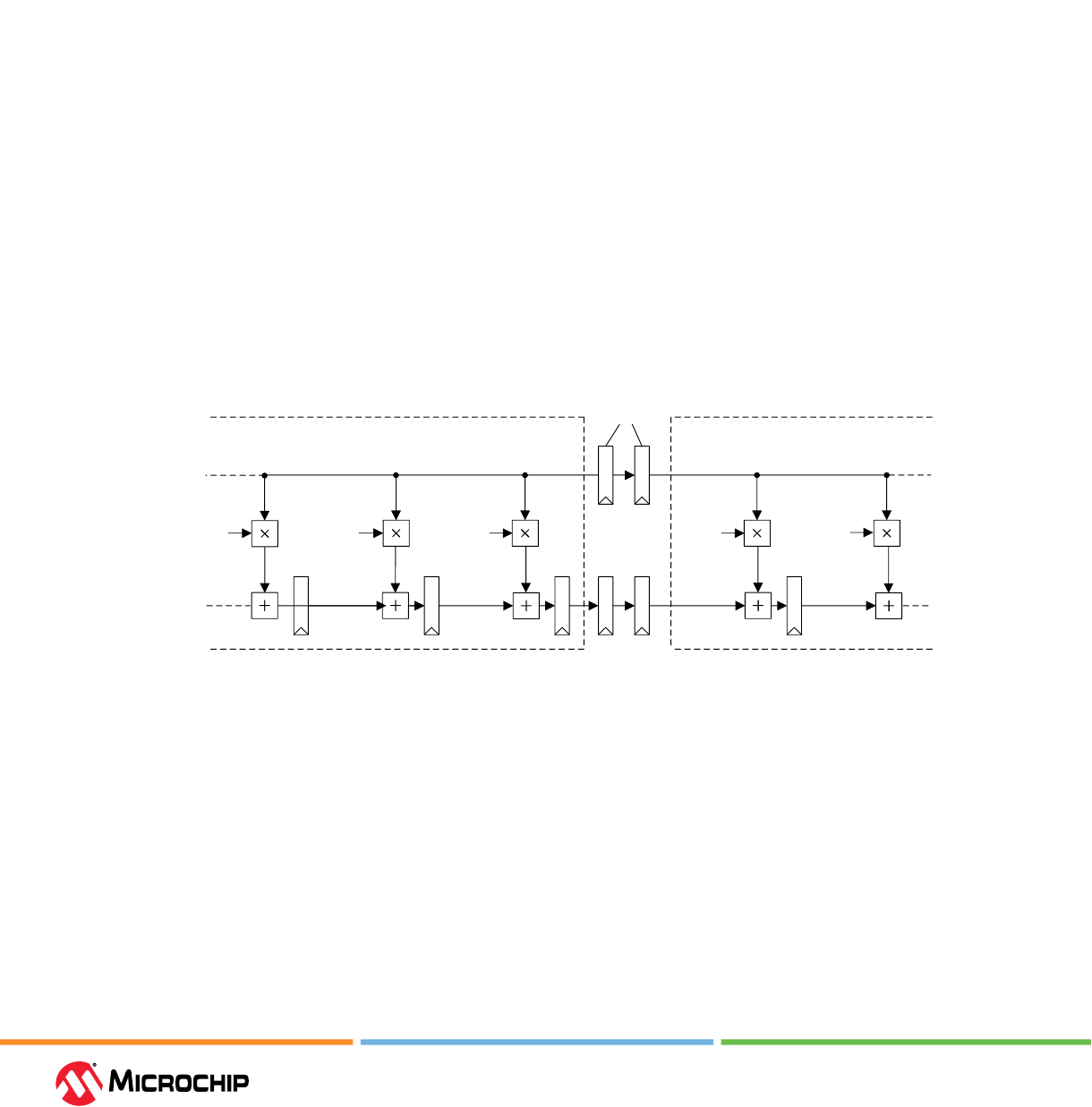
Math Blocks
User Guide
© 2023 Microchip Technology Inc. and its subsidiaries
DS60001725G - 66
for 16 xed coecient values. These coecients are loaded during device programming. The
coecient ROM content is accessed through ADDR[3:0] for multiplication.
• 18 ILs LUTs are used to implement a 2:1 mux for selecting the BCIN.
• 18 interface logic ip-ops are used to implement the B2 register, as shown in Figure 3-1. This
register is used in input delay chains for ltering applications.
Note: The coecient ROM is part of the interface logic associated with the Math block. It is dierent
from μPROM.
3.4 Cascading Math Blocks (Ask a Queson)
The Math blocks in each row cascade in a chain from left to right and terminate at the end of each
row. Fabric routing is required to extend the cascading chain from one row to another. The following
are the two options to connect cascading chains across multiple rows:
• 3.4.1. Wrap-Around to the Start of the Cascade Chain
• 3.4.2. Wrap-Around to the Inside of the Cascade Chain
3.4.1 Wrap-Around to the Start of the Cascade Chain (Ask a Queson)
The cascade chain output of one row is connected to the cascade chain input of another row
through fabric routing, with one or more pipeline registers added in the fabric to improve
performance. If latency is required at the output, additional compensating registers can be added on
the input side. The following gure shows an example implementation of a transpose FIR lter with
the cascade chain of one row being extended to the chain of another row through pipeline registers.
Figure 3-2. Wrap-Around of Cascade Chain Using Pipeline Registers in Fabric
C(i+3)
C(i+4)
C(i+2) C(i+1) C(i)
Physical Row/ k+1Physical Row/Column k
c
Pipelined
Register
3.4.2 Wrap-Around to the Inside of the Cascade Chain (Ask a Queson)
The cascade chain output of one row is connected to any adder input of another row. This type of
connection is useful when designing systolic or folded FIR lters. With this approach, there is no
need to insert compensating pipeline registers on the input side or create additional latency on the
output side.
The following gure shows an example implementation of a wrap-around to the inside of a cascade
chain.
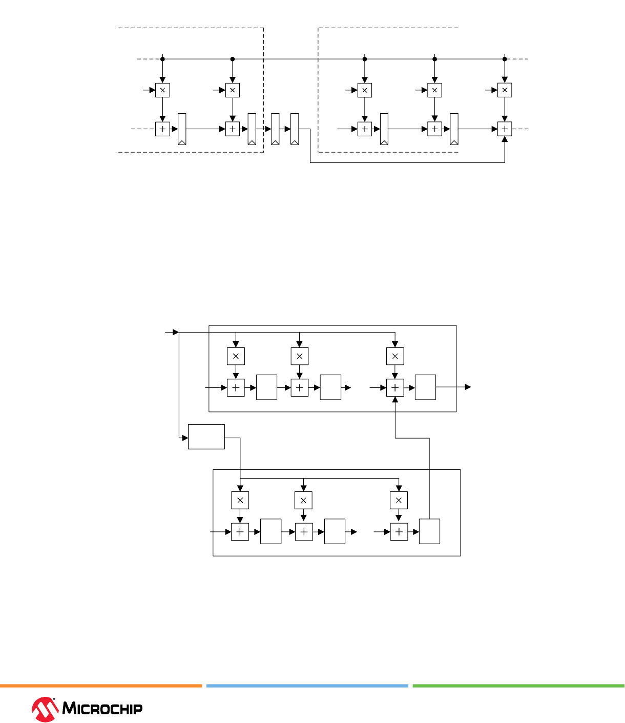
Math Blocks
User Guide
© 2023 Microchip Technology Inc. and its subsidiaries
DS60001725G - 67
Figure 3-3. Wrap-Around to Inside of Cascade Chain
C(i+3) C(i-1)C(i+2) C(i+1) C(i)
Physical Row k+1Physical Row k
0
3.4.2.1 Merging Mulple Cascade Chains (Ask a Queson)
Multiple cascade chains can be merged using either the C input of math block or adders constructed
in the fabric. Extra pipelined register must be added to adjust the latency.
The following gure shows multiple cascaded chains merged using a math block C input.
Figure 3-4. Merging Cascade Chains Using C Input
...
N-Stage Cascade Chain
-
z
1
-
z
1
-
z
1
z
-(n-1)
-
z
1
-
z
1
-
z
1
DIN
DOUT
ZERO
ZERO
N-Stage Cascade Chain
...
The following gure shows multiple cascaded chains merged with fabric adders.
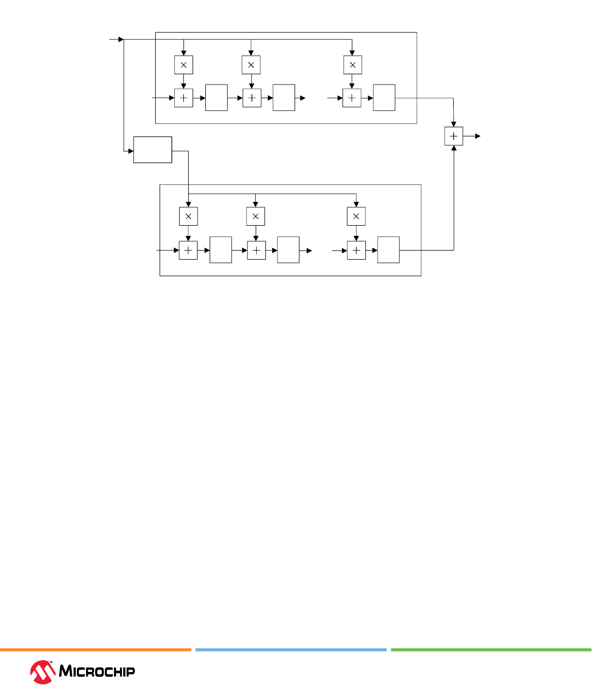
Math Blocks
User Guide
© 2023 Microchip Technology Inc. and its subsidiaries
DS60001725G - 68
Figure 3-5. Merging Cascade Chains Using Fabric Adders
N-Stage Cascade Chain
-
z
1
-
z
1
-
z
1
-
z
1
-
z
1
-
z
1
-
z
n
N-Stage Cascade Chain
DIN
ZERO
DOUT
ZERO
...
...
3.5 Operaonal Modes (Ask a Queson)
The Math block supports the following operational modes:
• 3.5.1. Normal Mode
• 3.5.2. DOTP Mode
• 3.5.3. SIMD Mode
3.5.1 Normal Mode (Ask a Queson)
Normal mode performs a 18-bit addition (pre-adder) and a 19 x 18 multiplication operation as per
the following output equation:
P[47:0] = ((B[17:0] ± D[17:0]) x A[17:0]) + C[47:0] + E[47:0] + CARRYIN
The following gure shows the functional block diagram of the Math block in normal mode.
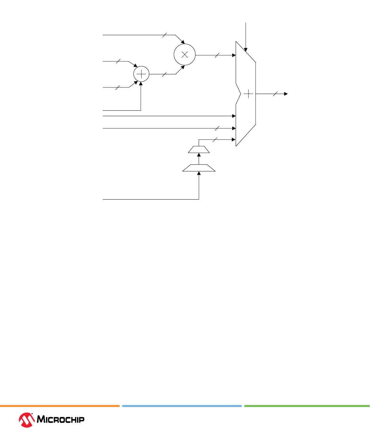
Math Blocks
User Guide
© 2023 Microchip Technology Inc. and its subsidiaries
DS60001725G - 69
Figure 3-6. Funconal Block Diagram of the Math Block in Normal Mode
A[17:0]
D[17:0]
CARRYIN
19
P[47:0]
18
B[17:0]
48
SUB
37
48
18
18
PSUB
C[47:0]
E[47:0]
00
11
01
>> 17
48
CDIN[47:0]
3.5.2 DOTP Mode (Ask a Queson)
DOTP mode computes the sum of two 10 x 9-bit multiplications. In this mode, the pre-adder is
split into two 9-bit adders. The two 9-bit pre-adders must be in the same mode, either addition or
subtraction.
In DOTP mode, the Math block implements the following output equation:
P[47:0] = ((B[8:0] ± D[8:0]) x A[17:9] ± (B[17:9] ± D[17:9]) x A[8:0]) x 2
9
+ C[47:0] + E[47:0] + CARRYIN
The following gure shows the functional block diagram of the Math block in DOTP mode.
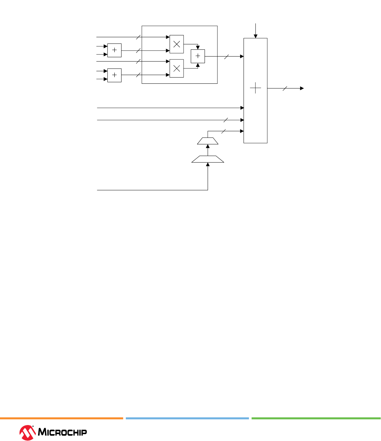
Math Blocks
User Guide
© 2023 Microchip Technology Inc. and its subsidiaries
DS60001725G - 70
Figure 3-7. Funconal Block Diagram of the Math Block in DOTP Mode
A[17:9]
B[8:0]
B[17:9]
48
49
SUB
P[47:0]
DOT Product Mode
D[8:0]
D[17:9]
10
A[8:0]
9
10
9
CARRYIN
48
C[47:0]
E[47:0]
00
11
01
>> 17
48
CDIN[47:0]
3.5.3 SIMD Mode (Ask a Queson)
In SIMD mode, the 18 x 19 multiplier operates as two independent 9 x 9 multipliers. It doubles the
number of multiplications for smaller widths (say 9 bits). It computes two independent 9 x 9-bit
multiplications using the 9-bit upper pre-adder. The lower pre-adder is not used (D[8:0] input must
be zero). The lower portion of the nal adder is not used, that is, E[17:0] is ignored and C[17:0] must
be zero. The ARSHFT17 input is also ignored in SIMD mode.
SIMD mode implements the following output equations:
P[17:0] = (B[8:0] x A[8:0]) + CARRYIN
P[47:18] = ((B[17:9] ± D[17:9]) x A[17:9]) + C[47:18] + E[47:18]
The following gure shows the functional block diagram of the Math block in SIMD mode.
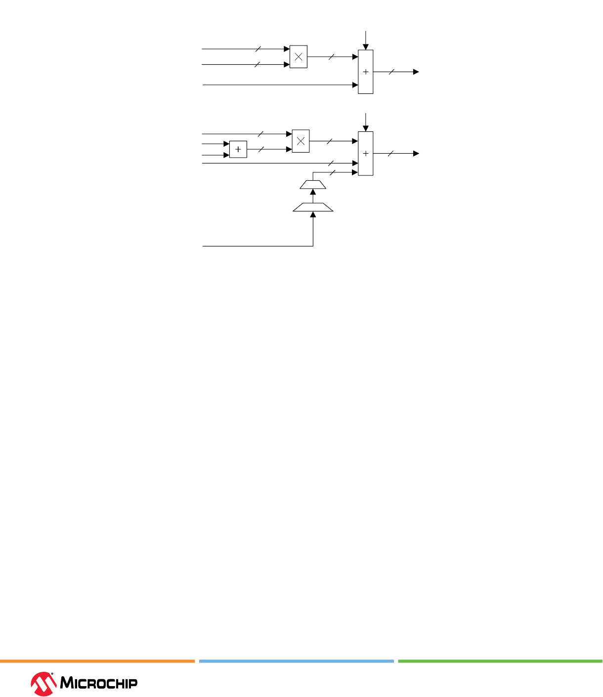
Math Blocks
User Guide
© 2023 Microchip Technology Inc. and its subsidiaries
DS60001725G - 71
Figure 3-8. Funconal Block Diagram of the Math Block in SIMD Mode
B[17:9]
30
C[47:18]
P[47:18]
A[17:9]
D[17:9]
10
SUB
19
A[8:0]
B[8:0]
SUB
CARRYIN
P[17:0]
18
9
9
9
E[47:0]
00
11
01
>> 17
48
CDIN[47:0]
3.6 Implementaon (Ask a Queson)
A Math block is implemented through one of the following methods:
• 3.6.1. RTL Inference
• 3.6.2. Math Block Macro
• 3.6.3. Use Models
3.6.1 RTL Inference (Ask a Queson)
Synplify Pro ME infers Math blocks and congures the appropriate modes automatically if the RTL
contains any specic multiply, multiply-accumulate, multiply-add, or multiply-subtract, pre-adder
multiply functions. Synthesis handles all the signal connections of the Math block to the rest of
the design and sets the correct values for the static signals needed to congure the appropriate
operational mode. Synplify Pro ME ties unused dynamic input signals to ground and provides
default values to unused static signals.
Synplify Pro ME automatically maps any multiplication functions with input widths of three or more
to Math blocks. For input widths less than three, Math blocks can be inferred by using synthesis
attribute (Syn_multstyle= “dsp”), the mapping of multiplication functions with input widths less than
three, (which are implemented in fabric logic by default), can be controlled by the synthesis attribute
(Syn_multstyle = “dsp”) if using Math blocks is preferred. The tool is also capable of cascading
multiple Math blocks if the function crosses the limits of a single Math block. For example, if the RTL
contains a 35 x 35 multiplication, synthesis implements this block using four Math blocks cascaded
in a chain.
Synplify Pro ME also has the capability to utilize the input and output registers inside the Math
block boundary, provided they are in the same clock domain. If the registers are in dierent clock
domains, the clock that drives the output register has priority, and all registers driven by that clock
are placed in the Math block. If the outputs are unregistered and the inputs are registered but
not all on the same clock domain, the input registers with the larger input have priority and are
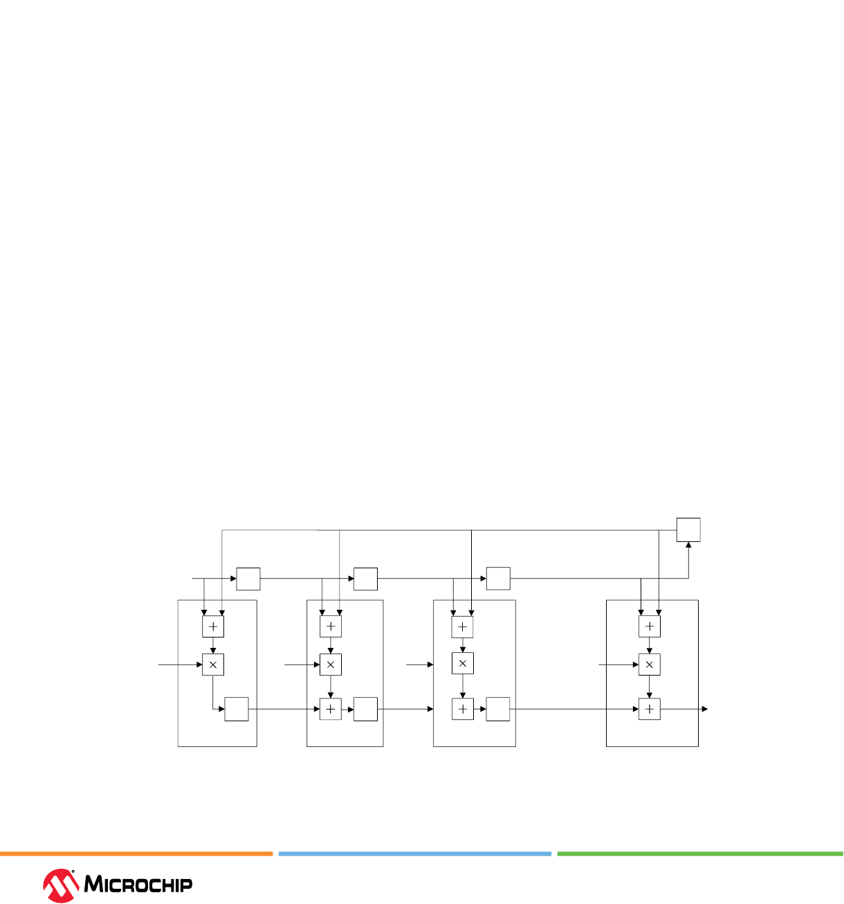
Math Blocks
User Guide
© 2023 Microchip Technology Inc. and its subsidiaries
DS60001725G - 72
placed in the Math block. The synthesis tool supports inferencing of Math block components across
hierarchical boundaries. In this case even if the multipliers, input registers, output registers, and
adders/subtractors are present at dierent levels of a design's hierarchy, they can be placed into
the same Math block. For more information about Math block inference by Synplify Pro ME, see
Inferring PolarFire MACC Blocks Application Note.
3.6.2 Math Block Macro (Ask a Queson)
The Math block macro is available in the Libero SoC > IP Catalog as a component that can be used
directly in an HDL le or instantiated in SmartDesign. Math block has the following two macros.
• MACC_PA (MACC with Pre-Adder)
• MACC_PA_BC_ROM (MACC with Pre-Adder, BCOUT Register, and Coecient ROM)
For more information about conguring Math block macro, see 5.3. Math Block Macro.
3.6.3 Use Models (Ask a Queson)
Math blocks can be used in a wide variety of DSP applications and this section describes the
following use models:
• 3.6.3.1. Symmetric FIR Filter
• 3.6.3.2. 9 x 9 Systolic FIR Filter
• 3.6.3.3. 9 x 9 Symmetric FIR Filter
• 3.6.3.4. 9 x 9 Complex Multiplier
• 3.6.3.5. Non-Pipelined 35 x 35 Multiplier Using Cascade Chain
• 3.6.3.6. Pipelined 35 x 35 Multiplier Using Cascade Chain
• 3.6.3.7. Non-Pipelined 35 x 35 Multiplier Using Fabric Adders
• 3.6.3.8. Extension Adder
3.6.3.1 Symmetric FIR Filter (Ask a Queson)
In symmetrical FIR lters, the coecients are symmetrical. Because of the symmetry, an M-tap FIR
lter can be implemented using M/2 Math blocks. The Math block pre-adder is used to add the input
signal feeding the symmetric lter coecients, as shown in the following gure.
Figure 3-9. Symmetric FIR Filter Implementaon
x(n+M/2 –
c(0)
-
-
c(1)
-
c(2) c(M/2
-
1)
y(n)
...
-
Math BLock 1 Math BLock 2 Math BLock 3
Math Block M/2
z
2
z
1
z
1
z
1
z
-1
z
-2
z
-2
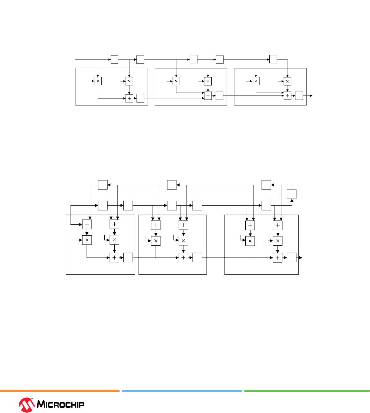
Math Blocks
User Guide
© 2023 Microchip Technology Inc. and its subsidiaries
DS60001725G - 73
Anti-symmetric FIR lters can also be implemented in the same way, but with the pre-adder
congured to subtract the input signals feeding the anti-symmetric lter coecients, as shown in
Figure 3-10.
3.6.3.2 9 x 9 Systolic FIR Filter (Ask a Queson)
A 9 x 9 systolic FIR lter can be implemented using the 9 x 9 DOTP mode of the Math block, see
Figure 3-10. In DOTP mode, two multipliers share the same output register. As a result, the latencies
have to be adjusted properly on the input side to achieve correct lter operation.
Figure 3-10. 9 x 9 Systolic FIR Filter
x(n+M-1)
c(0)
Z
-1
Z
-1
c(1)
c(2)
Z
-1
Z
-1
Z
-2
c(3)
Math Block 1
Math Block 2
Z
-2
c(n-1)
Z
-1
Z
-1
c(n)
Math Block n
...
y(n)
3.6.3.3 9 x 9 Symmetric FIR Filter (Ask a Queson)
A 9 x 9 symmetric FIR lter can be implemented by using the 9 x 9 DOTP mode with the Math block
pre-adder congured as two 9-bit pre-adders. The following gure shows an example of a 9 x 9
symmetric FIR lter for M number (divisible by 4) of taps.
Figure 3-11. 9 x 9 Symmetric FIR Filter
x(n+M/4-1)
Z
-1
Z
-2
c(1)
y(n –
Z
-1
Z
-1
c(0)
Z
-1
Z
-1
Z
-2
c(3)
Z
-1
c(2)
Z
-1
Z
-1
c(M/2 –
Z
-1
c(M/2 –
Z
-1
x(n-M/2)
Math Block 1 Math Block M/4
x(n-3M/4)
Math Block 2
...
3.6.3.4 9 x 9 Complex Mulplier (Ask a Queson)
To implement a 9 x 9 complex multiplier, 2 Math blocks and an additional 2's complement logic (in
the fabric) are required. The 2's complement logic in the fabric is needed for negating the Q input, as
shown in Figure 3-12, and this logic consumes minimal fabric resources.
For two complex numbers, X + jY and P + jQ, the complex multiplication is:
Multiplication result = real part + imaginary part = (PX – QY) + j (PY + QX).
The real part (PX - QY) requires -Q for the multiplication result. In 2's complement arithmetic this
value can be computed using the 1's complement of Q and adding the Y using the C input (-Q = ~Q +
1).
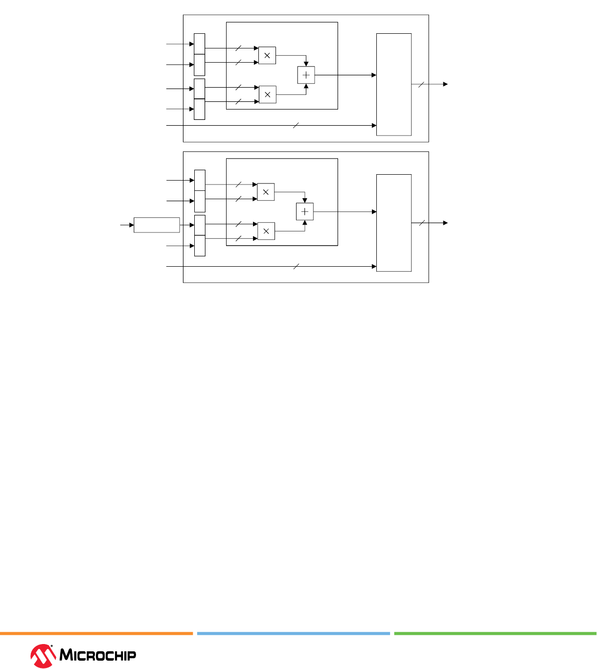
Math Blocks
User Guide
© 2023 Microchip Technology Inc. and its subsidiaries
DS60001725G - 74
Real part = P x X + (~Q) x Y + Y.
Figure 3-12. 9-Bit Complex Mulplicaon Using DOTP Mode
3-Input
Adder
X
Y
P
Q
<< 9
Dot Product Mode
Math Block 1
3-Input
Adder
<< 9
Dot Product Mode
Math Block 2
C[47:0] = Zeroes
48
48
X
Y
Q
P
1's Complement
Logic
C[47:19] = ZEROS
C[9:0] = ZEROS
C[18:10] = Y
9
9
9
9
48
48
PY + QX
(Imaginary Value)
PX - QY
(Real Value)
A H B L B H A L
A H B L B H A L
9
9
9
9
3.6.3.5 Non-Pipelined 35 x 35 Mulplier Using Cascade Chain (Ask a Queson)
A 35 x 35 multiplier is useful for applications requiring more than 18-bit precision. A non-pipelined
implementation is typically used for low-speed applications. A non-pipelined 35 x 35 multiplier can
be implemented using the cascaded Math blocks in a single row. Figure 3-13 shows an example of
such an implementation.
The inputs are assumed to be A[34:0] and B[34:0] with a product of P[69:0].
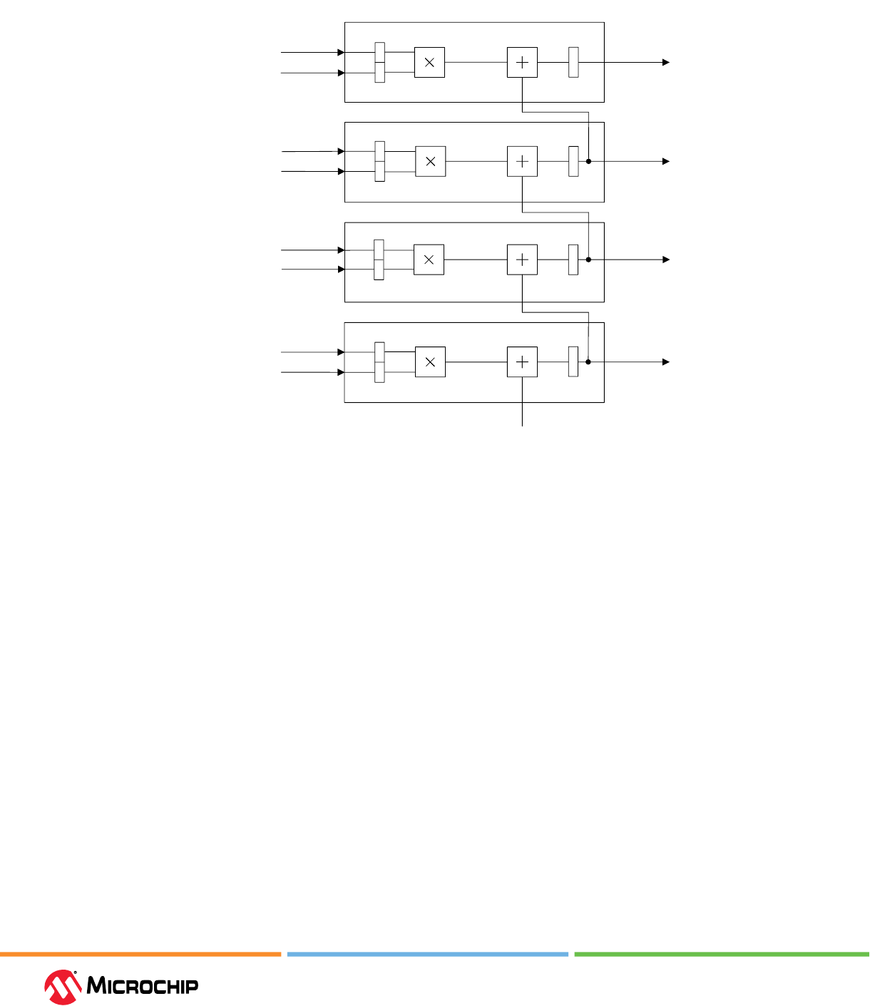
Math Blocks
User Guide
© 2023 Microchip Technology Inc. and its subsidiaries
DS60001725G - 75
Figure 3-13. Non-Pipelined Implementaon Using Cascade Chain
B
H
[17:0] = B[34:17]
A
L
[17:0] = {0, A[16:0]}
B
H
[17:0] = B[34:17]
A
H
[17:0] = A[34:17]
B
L
[17:0] = {0, B[16:0]}
A
L
[17:0] = {0, A[16:0]}
B
L
[17:0] = {0, B[16:0]}
A
H
[17:0] = A[34:17]
>>17
P[69:34]
P[16:0]
P[33:17]
Unconnected
0
>>17
3.6.3.6 Pipelined 35 x 35 Mulplier Using Cascade Chain (Ask a Queson)
Math blocks have IL registers accessible to all input and output ports. To implement pipelined
multipliers, these IL registers are added to the input or output side of the non-pipelined
implementation. These registers are needed for balancing the pipeline latency.
The following gure shows a typical 35 x 35 multiplier implementation with fabric pipeline registers.
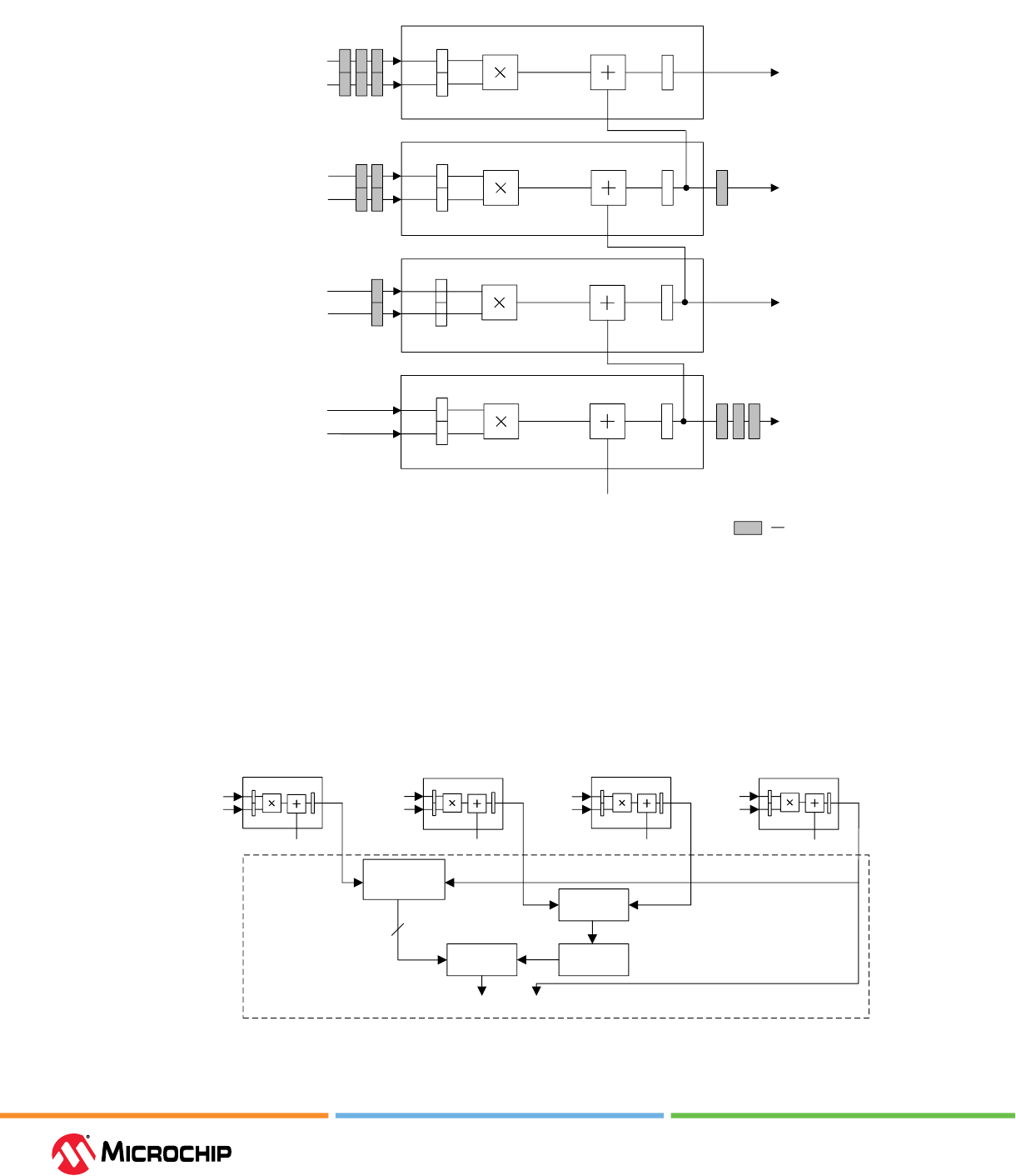
Math Blocks
User Guide
© 2023 Microchip Technology Inc. and its subsidiaries
DS60001725G - 76
Figure 3-14. Pipelined Implementaon Using Cascade Chain
B
H
[17:0] = B[34:17]
A
L
[17:0] = {0, A[16:0]}
B
H
[17:0] = B[34:17]
A
H
[17:0] = A[34:17]
B
L
[17:0] = {0, B[16:0]}
A
L
[17:0] = {0, A[16:0]}
B
L
[17:0] = {0, B[16:0]}
A
H
[17:0] = A[34:17]
>>17
P[69:34]
P[16:0]
P[33:17]
Unconnected
0
>>17
Fabric Registers
3.6.3.7 Non-Pipelined 35 x 35 Mulplier Using Fabric Adders (Ask a Queson)
A non-pipelined 35 x 35 multiplier can be implemented using fabric adders. This reduces the output
latency compared to the non-pipelined cascade-chain implementation.
The following gure shows the block diagram of the 35 x 35 multiply using fabric adders.
Figure 3-15. 35 x 35 Mulply Using Fabric Adders
B[34:17]
A[34:17]
B[16:0]
A[34:17]
B[34:17]
A[16:0]
B[16:0]
A[16:0]
0
0 0
Concatenate
35-bit
Adder
53-bit
Adder
Sign Extend
P2[33:17]
P2[16:0]
P[16:0]P[69:17]
P0[33:0]
P1[33:0]
P1[33:0]
P2[33:0]
53-bit
Math Block 1
Math Block 2
Math Block 3
Math Block 4
Fabric
0
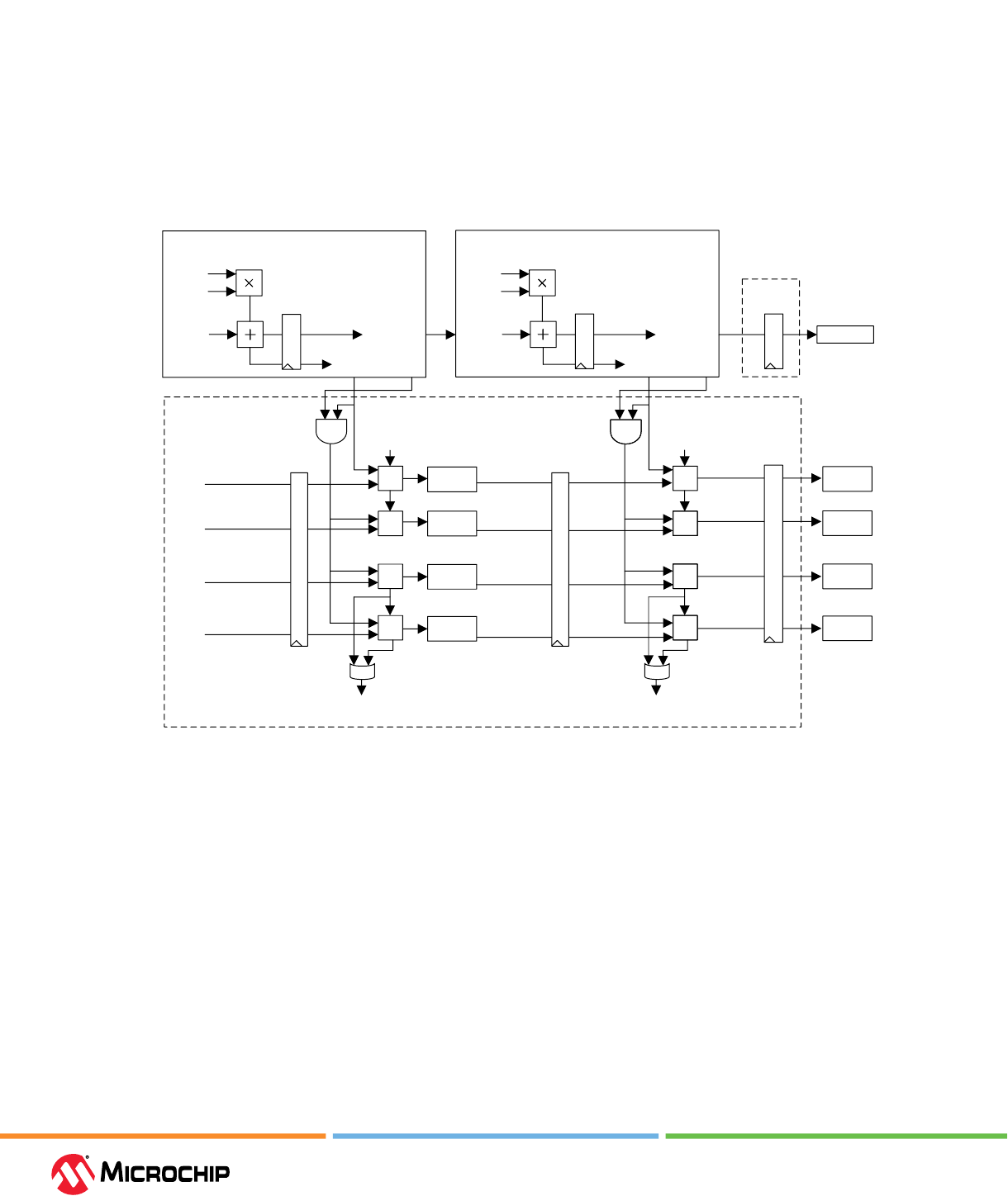
Math Blocks
User Guide
© 2023 Microchip Technology Inc. and its subsidiaries
DS60001725G - 77
3.6.3.8 Extension Adder (Ask a Queson)
A Math block's adder/accumulator width can be extended using fabric logic. Figure 3-16 and Figure
3-17 show example implementations of 2-input and 3-input extension adders in fabric. In this
extension adder, the MSb bits, P[47], C[47], and E[47] are not treated as sign bits. Instead, P[n-1]
represents the sign bit. The static input EXT_SEL is set to 1 causing the appropriate signal to appear
on each Math block's OVFL_CARRYOUT output.
The following gure shows a case where input C = 0, and input E is used for the cascade chain.
Figure 3-16. Extension of 2-Input Adder in Fabric
OVFL
P[48]
+
+
+
...
P[49]
+
0
P[47:0]
Math Block
P[47:0]
OVFL_EXT
P[47]
P[n-2]
P[n-1]
OVFL
+
+
+
...
+
0
P[48]
P[49]
P[n-2]
P[n-1]
Math Block
E[47:0]
A[17:0]
B[17:0]
P[47:0]
OVFL_EXT
P[47]
Fabric
E[47:0]
A[17:0]
B[17:0]
Fabric
The following gure shows a case where both inputs C and E are used.
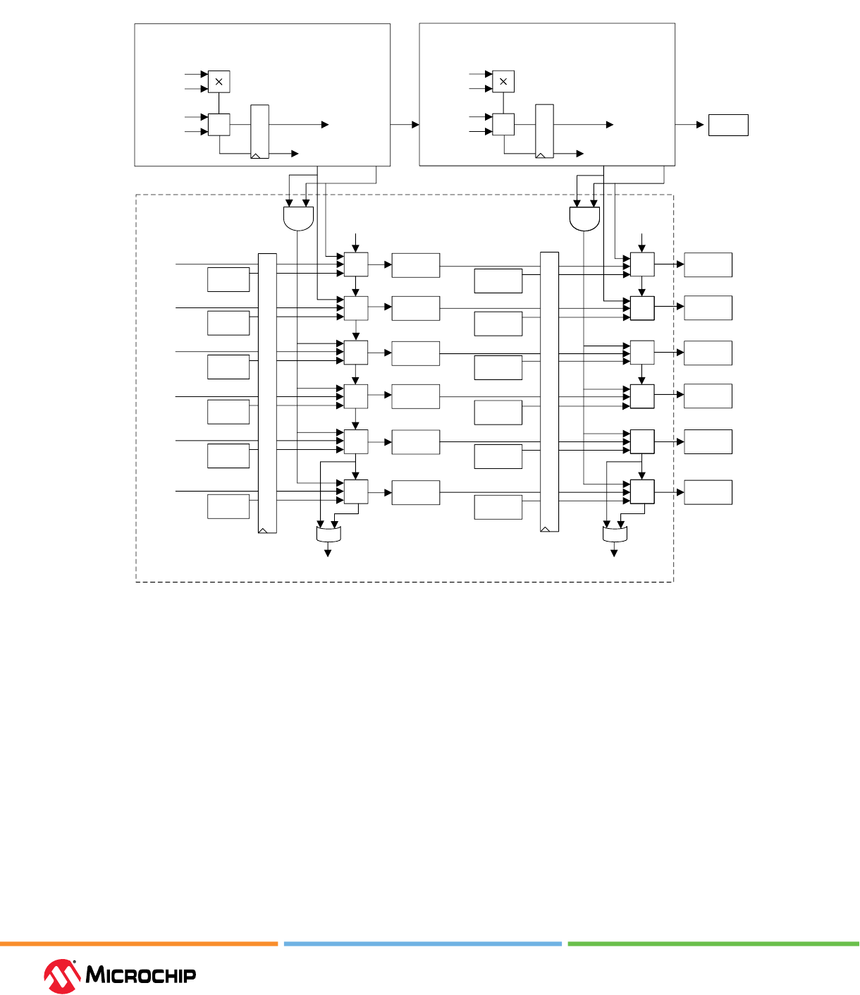
Math Blocks
User Guide
© 2023 Microchip Technology Inc. and its subsidiaries
DS60001725G - 78
Figure 3-17. Extension of 3-Input Adder in Fabric
C[47]
C[48]
C[49]
C[n-3]
C[n-2]
C[n-1]
OVFL
Fabric
P[47]
+
+
+
P[48]
+
Math Block
E[46:0]
A[17:0]
B[17:0]
P[46:0]
OVFL_EXT
P[47]
P[n-2]
P[n-1]
OVFL
+
+
+
...
+
P[47]
P[48]
P[n-2]
P[n-1]
Math Block
C[46:0]
A[17:0]
B[17:0]
P[46:0]
OVFL_EXT
P[47]
E[46:0]
C[46:0]
P[49]
+
P[n-3]
+
+
...
+
P[49]
P[n-3]
C[47]
C[48]
C[49]
C[n-3]
C[n-2]
C[n-1]
0 0
+
+
P[46:0]

Appendix: Supported Memory File Formats for LSRAM and μSRAM
User Guide
© 2023 Microchip Technology Inc. and its subsidiaries
DS60001725G - 79
4. Appendix: Supported Memory File Formats for LSRAM and μSRAM (Ask
a Queson)
Microchip supports Intel-Hex, Motorola-S, Simple-Hex, and Binary le formats.
Note: Implementation of these formats interpret data sets in bytes. If the memory width is 7 bits,
then every eighth bit in the data set is ignored. If the data width is 9 bits, two bytes are assigned to
each memory address, and the upper 7 bits of each 2 byte pair are ignored. For more information,
see 4.1. Write Port Width Alignment
INTEL-HEX
Intel-Hex is an industry standard le format created by Intel. File extensions for these les are .hex
and .ihx.
Memory contents are stored in ASCII les using hexadecimal characters. Each le contains a series
of records (lines of text) delimited by new line, '\n', characters and each record starts with a ':'
character. For more information about this format, see the Intel-Hex Record Format Specication.
The Intel-Hex record is composed of ve elds and is arranged as:
:llaaaatt[dd...]cc
Where:
• :—start code of every Intel-Hex record.
• ll—byte count of the data eld.
• aaaa—16-bit address of the beginning of the memory position for the data. Address is big
Endian.
• tt—record type, denes the data eld:
– 00—data record.
– 01—end of le record.
– 02—extended segment address record.
– 03—start segment address record (ignored by Microchip SoC tools).
– 04—extended linear address record.
– 05—start linear address record (ignored by Microchip SoC tools).
• [dd...]—sequence of n bytes of the data. n is equivalent to what was specied in the ll eld.
• cc—checksum of count, address, and data.
Example Intel-Hex record:
:0300300002337A1E
Note: Congurator organizes data according to big Endian sequence. Intel-Hex format requires
byte-aligned port widths. For more information, see 4.1. Write Port Width Alignment.
Motorola S-Record
Motorola S-Record is an industry standard le format created by Motorola. The le extension for
these les is .s.
This format uses ASCII les, hex characters, and records to specify memory content similar to the
Intel-Hex format. See the Motorola S-record description document for more information about this
format. The RAM Content Manager uses only the S1 through S3 record types. The other record types
are ignored.
The major dierence between Intel-Hex and Motorola-S is the record formats and extra error
checking features that are incorporated into the Motorola S-record.

Appendix: Supported Memory File Formats for LSRAM and μSRAM
User Guide
© 2023 Microchip Technology Inc. and its subsidiaries
DS60001725G - 80
In both formats, memory content is specied by providing a starting address and a data set. The
upper bits of the data set are loaded into the starting address and leftovers overow into the
adjacent addresses until the entire data set has been used.
The Motorola S-record is composed of six elds and arranged as follows:
Stllaaaa[dd...]cc
Where:
• S—start code of every Motorola S-record.
• t—record type, denes the data eld.
• ll—byte count of the data eld.
• aaaa—16-bit address at the beginning of the memory position for the data. Address is big Endian.
• [dd...]—sequence of n bytes of the data; n is equivalent to what was specied in the ll eld.
• cc—checksum of count, address, and data.
Example Motorola S-record:
S10a0000112233445566778899FFFA
Note: Congurator organizes data according to big Endian sequence. Motorola-S format requires
byte-aligned port widths. For more information, see 4.1. Write Port Width Alignment.
Simple-Hex
Simple-Hex is a format created by Autodesk. SHX les are used for environment enabling designs of
2D and 3D projects for engineering purposes. These les end with an SHX extension (for example,
file2.shx or file3.shx).
The Simple-Hex record is arranged as follows:
0:2000D9B8
Where, the colon (:) separates the address from the data.
Note: Congurator organizes data according to little Endian sequence. Simple-Hex format requires
byte-aligned port widths. For more information, see 4.1. Write Port Width Alignment.
Binary
Binary les consist of a sequence of bytes, with the binary digits (bits) grouped in eights. Files consist
of 0s and 1s and end with a BIN extension. For example, file2.bin or file3.bin.
The Binary record is composed as follows:
001100101010101010010010
Note: Congurator organizes data according to little Endian sequence. Binary format requires byte-
aligned port widths. For more information, see 4.1. Write Port Width Alignment.
MEMFILE (RAM Content Manager output le)
Transfer of RAM data (from the RAM Content Manager) to test equipment is accomplished through
MEM les.
The contents of RAM is rst organized into the logical layer and then reorganized to t the hardware
layer. Then it is stored in MEM les that are read by other systems and used for testing. The MEM
les are named according to the logical structure of the RAM elements created by the congurator.
In this scheme, the highest order RAM blocks are named CORE_R0C0.mem, where R stands for
row and C stands for column. For multiple RAM blocks, the naming continues with CORE_R0C1,
CORE_R0C2, CORE_R1C0, and so on.
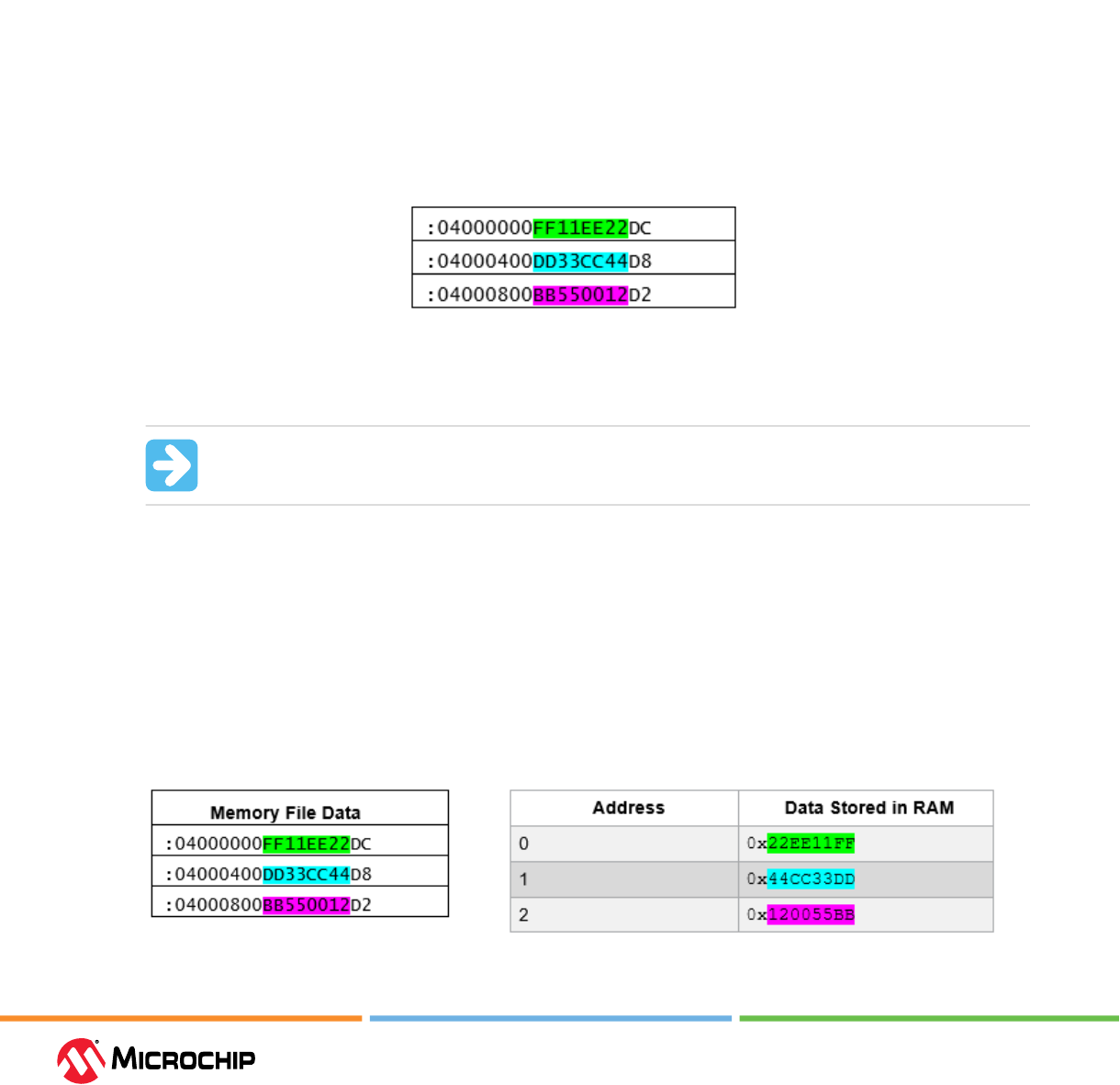
Appendix: Supported Memory File Formats for LSRAM and μSRAM
User Guide
© 2023 Microchip Technology Inc. and its subsidiaries
DS60001725G - 81
The data intended for the RAM is stored as ASCII 1s and 0s within the le. Each memory address
occupies one line. Words from the logical layer blocks are concatenated or split in order to make
them t eciently within the hardware blocks. If the logical layer width is less than the hardware
layer, two or more logical layer words are concatenated to form one hardware layer word. In this
case, the lowest bits of the hardware word are made up of the lower address data bits from the
logical layer. If the logical layer width is more than the hardware layer, the words are split, placing
the lower bits in lower addresses.
If the logical layer words do not t cleanly into the hardware layer words, the most signicant bit of
the hardware layer words is not used and defaulted to zero. This is also done when the logical layer
width is 1 in order to avoid having leftover memory at the end of the hardware block.
4.1 Write Port Width Alignment (Ask a Queson)
The Microchip implementation of these formats interprets data sets in bytes. The implementation
used is the same for all memory formats. The following examples show how data in a memory le is
interpreted for dierent write port widths of memory.
The following gure shows data in Intel HEX memory le format. The same data is assumed to be
used to initialize RAM in all examples.
Figure 4-1. Memory File Data—Intel HEX Memory File Format
The Hex data from the memory le is converted into binary and read by the tool as a stream of bits.
Based on the memory port width, the required number of bits for each address location in RAM is
taken from the stream of bits.
Important: The required number of bits taken from the stream of bits for each address
location is always a multiple of 8 (byte).
4.1.1 Write Port Widths Aligned on Byte Boundary (Ask a Queson)
The following examples show how data from a memory le is stored in RAM when memory port
widths are a multiple of a byte (aligned on a byte boundary).
4.1.1.1 32-Bit Write Port Width (Ask a Queson)
When the memory write port width is 32 bits, which is aligned on a byte boundary, the tool uses
32 bits from the binary stream for each 32-bit word in the RAM. The resulting data stored in RAM is
shown in the following gure.
Figure 4-2. Data in RAM—32-Bit Write Port Width Aligned on Byte Boundary
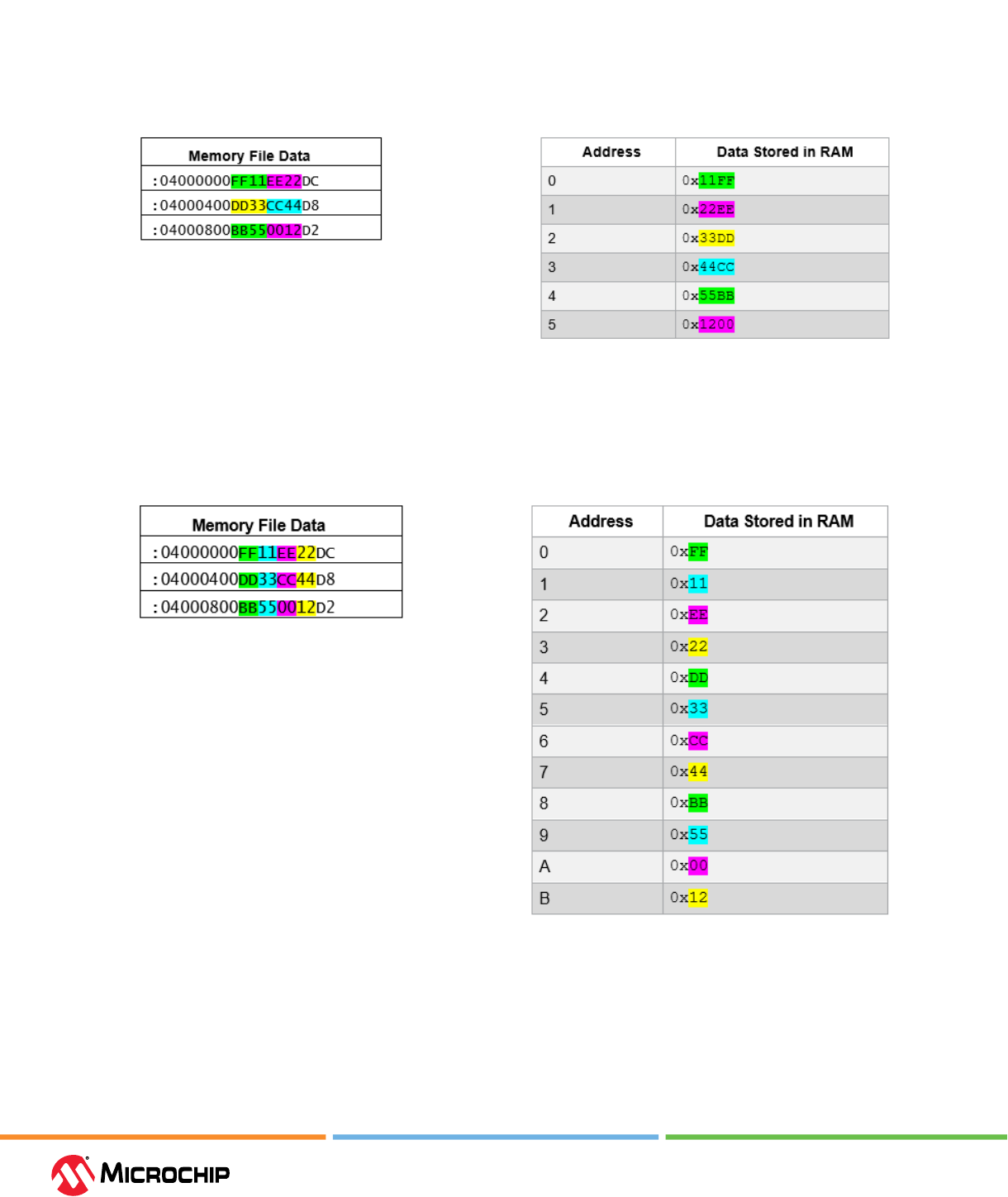
Appendix: Supported Memory File Formats for LSRAM and μSRAM
User Guide
© 2023 Microchip Technology Inc. and its subsidiaries
DS60001725G - 82
4.1.1.2 16-bit Write Port Width (Ask a Queson)
When the memory write port width is 16 bits, which is aligned on a byte boundary, the tool uses
16 bits from the binary stream for each 16-bit word in the RAM. The resulting data stored in RAM is
shown in the following gure.
Figure 4-3. Data in RAM - 16-bit Write Port Width Aligned on Byte Boundary
4.1.1.3 8-bit Write Port Width (Ask a Queson)
When the memory write port width is 8 bits, which is aligned on a byte boundary, the tool uses 8 bits
from the binary stream for each 8-bit word in the RAM. The resulting data stored in RAM is shown in
the following gure.
Figure 4-4. Data in RAM - 8-bit Write Port Width Aligned on Byte Boundary
4.1.2 Write Port Widths Not Aligned on Byte Boundary (Ask a Queson)
The following examples show how data from a memory le is stored in RAM when memory port
widths are not a multiple of a byte.
4.1.2.1 9-bit Write Port Width (Ask a Queson)
When the memory write port width is 9 bits, which is not aligned on a byte boundary, the tool uses
16 bits from the binary stream for each 9-bit word. The tool ignores the upper 7 bits of each 16 bits
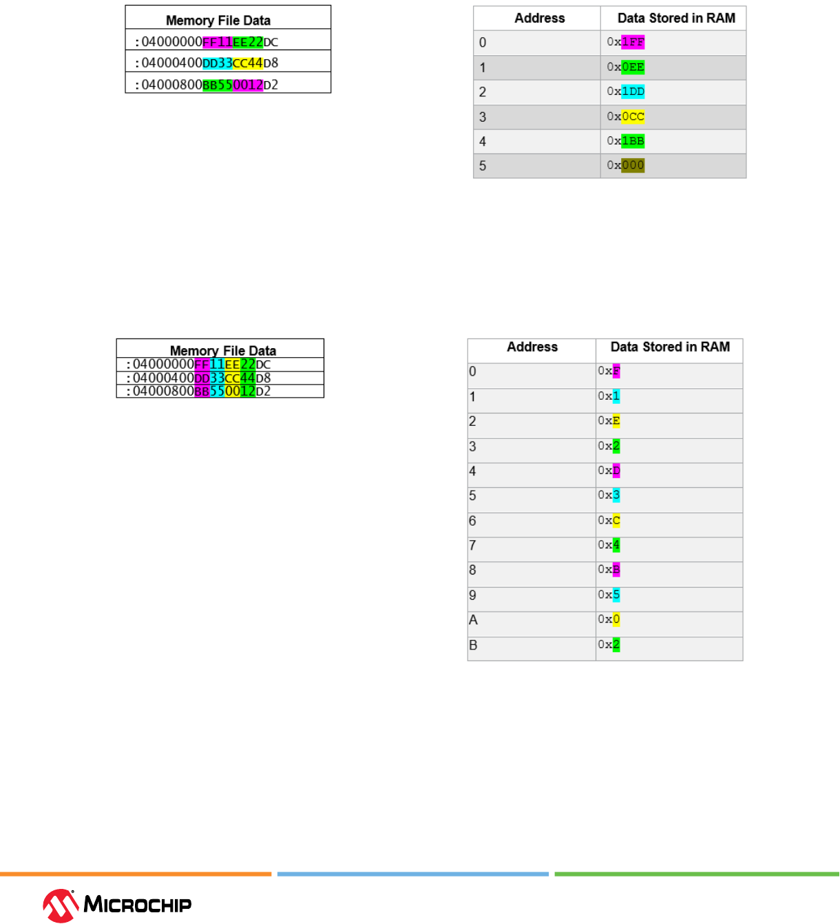
Appendix: Supported Memory File Formats for LSRAM and μSRAM
User Guide
© 2023 Microchip Technology Inc. and its subsidiaries
DS60001725G - 83
when processing the memory le data. The resulting data stored in RAM is shown in the following
gure.
Figure 4-5. Data in RAM - 9-bit Write Port Width Not Aligned on Byte Boundary
4.1.2.2 4-Bit Write Port Width (Ask a Queson)
When the memory write port width is 4 bits, which is not aligned on a byte boundary, the tool uses
8 bits from the binary stream for each 4-bit word. The tool ignores the upper 4 bits of each 8 bits
when processing the memory le data. The resulting data stored in RAM is shown in the following
gure.
Figure 4-6. Data in RAM—4-Bit Write Port Width Not Aligned on Byte Boundary
4.1.3 Specifying Data in Memory File (Ask a Queson)
If all the bits in the memory le are relevant, take steps to avoid bits from being ignored when the
write port width is not aligned on a byte boundary. The following examples describe how to specify
data in memory le so that the tool does not ignore bits. To avoid bits from being ignored, convert
the hexadecimal data intended to initialize RAM into binary stream of bits, and then pad (insert)
zeros based on the port width so that resulting data is byte-aligned, as described in the following
sections.
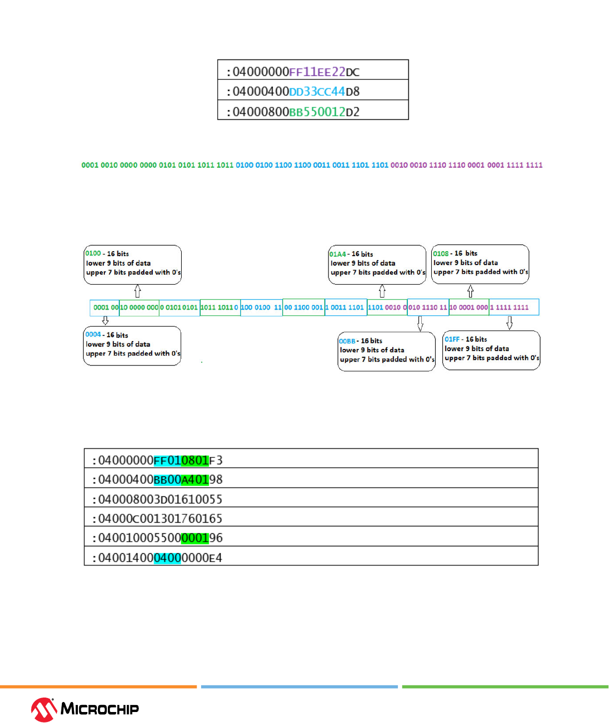
Appendix: Supported Memory File Formats for LSRAM and μSRAM
User Guide
© 2023 Microchip Technology Inc. and its subsidiaries
DS60001725G - 84
4.1.3.1 9-bit Write Port Width (Ask a Queson)
Consider the following Intel HEX memory le.
Figure 4-7. Memory File Data - Intel HEX Memory File
The binary stream of bits for above memory le data is:
If the memory port width is 9 bits, you must pad 7 zeros to every 9 bits of data from the binary
stream to create 16 bits (byte-aligned), as shown in the following gure.
Figure 4-8. Padding Zeros to Create 16 Bits
The following gure shows the equivalent memory le data padded with zeros to achieve a 9-bit
write port width.
Figure 4-9. Equivalent Memory File Data Padded with Zeros (9-bit Write Port Width)
When the tool parses the above memory le data (padded with zeros), the tool converts the data to
binary and reads it as a stream of bits. If the port width is 9 bits, the tool reads 16 bits (byte-aligned),
ignores the upper 7 bits, and stores the lower 9 bits of actual data in RAM, as shown in the following
table.
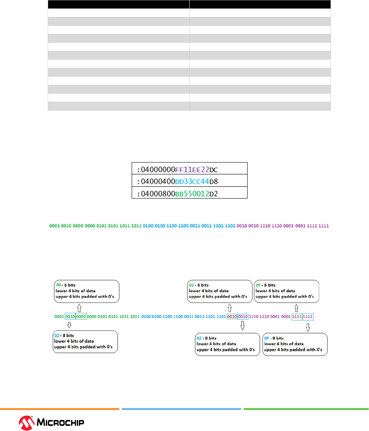
Appendix: Supported Memory File Formats for LSRAM and μSRAM
User Guide
© 2023 Microchip Technology Inc. and its subsidiaries
DS60001725G - 85
Table 4-1. 16-bit Write Port Width
Address Data
0
0x1FF
1
0x108
2
0x0BB
3
0x1A4
4
0x13D
5
0x061
6
0x113
7
0x176
8
0x055
9
0x100
A
0x004
B
0x000
4.1.3.2 4-Bit Write Port Width (Ask a Queson)
Enter a short description of your concept here (optional).
Consider the following Intel HEX memory le.
Figure 4-10. Memory File Data—Intel HEX Memory File
The binary stream of bits for above memory le data is:
If the memory port width is 4 bits, the tool reads 8 bits at a time from the binary stream above. For
the 8 bits, you must pad zeros for the upper 4 bits and specify the actual data in the lower 4 bits, as
shown in the following gure.
Figure 4-11. Padding Zeros for the Upper 4 Bits and Specifying Data in the Lower 4 Bits
The following gure shows the equivalent memory le data padded with zeros to achieve a 4-bit
write port width.
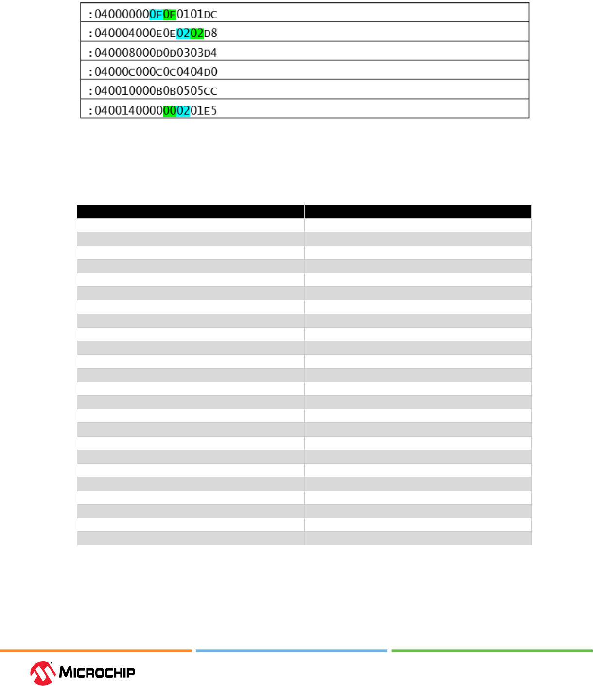
Appendix: Supported Memory File Formats for LSRAM and μSRAM
User Guide
© 2023 Microchip Technology Inc. and its subsidiaries
DS60001725G - 86
Figure 4-12. Equivalent Memory File Data Padded with Zeros (4-bit Write Port Width)
When the tool parses the above memory le data (padded with zeros), it converts the data to binary
and reads it as a stream of bits. If the port width is 4 bits, the tool reads 8 bits (byte-aligned), ignores
the upper 4 bits of actual data, and stores the lower 4 bits of actual data in RAM, as listed in the
following table.
Table 4-2. 16-bit Write Port Width
Address Data
0
0xF
1
0xF
2
0x1
3
0x1
4
0xE
5
0xE
6
0x2
7
0x2
8
0xD
9
0xD
A
0x3
B
0x3
C
0xC
D
0xC
E
0x4
F
0x4
10
0xB
11
0xB
12
0x5
13
0x5
14
0x0
15
0x0
16
0x2
17
0x1
Note: x1 and x2 port widths are handled using the same technique of padding zeros. You always
zero pad to the next 8-bit-width increment (8, 16, 24, and so on). If a write port width is not aligned
on a byte boundary, the following message appears.
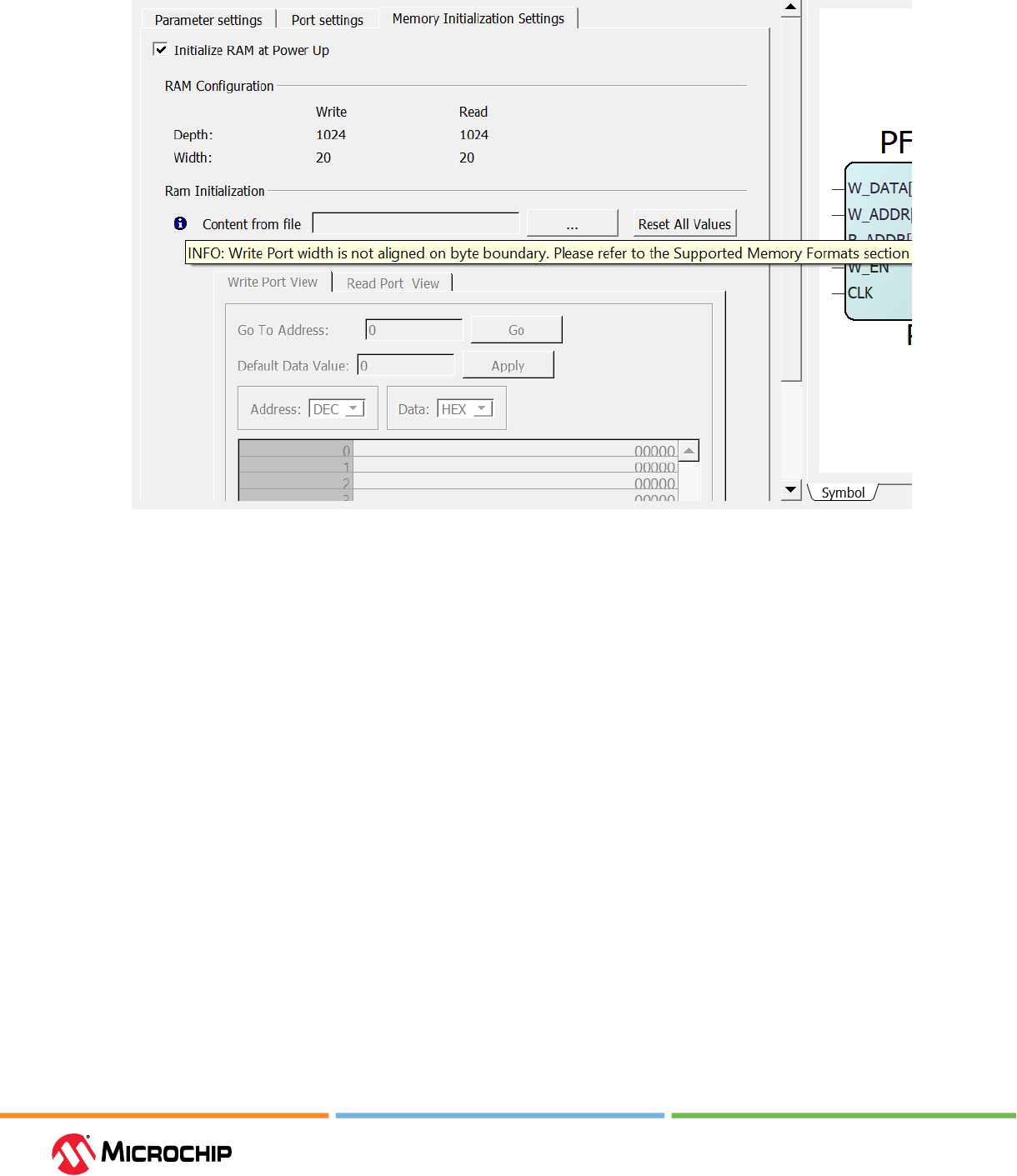
Appendix: Supported Memory File Formats for LSRAM and μSRAM
User Guide
© 2023 Microchip Technology Inc. and its subsidiaries
DS60001725G - 87
Figure 4-13. Message when a Write Port Width is Not Aligned on a Byte Boundary

Appendix: Macro Conguraon
User Guide
© 2023 Microchip Technology Inc. and its subsidiaries
DS60001725G - 88
5. Appendix: Macro Conguraon (Ask a Queson)
This section describes the conguration of LSRAM, µSRAM, and Math block macros.
5.1 LSRAM Macro (Ask a Queson)
The LSRAM macro (RAM1K20) in the Libero SoC IP macro library can be used directly to instantiate
the LSRAM block in the design. The LSRAM block must be congured with appropriate values
of the static signals. Instantiating LSRAM primitives in a design is not recommended. For the
recommended methods of instantiating memory in a user design, see 2.1.3.3. LSRAM Memory
Macro. The following gure shows the LSRAM macro (RAM1K20).
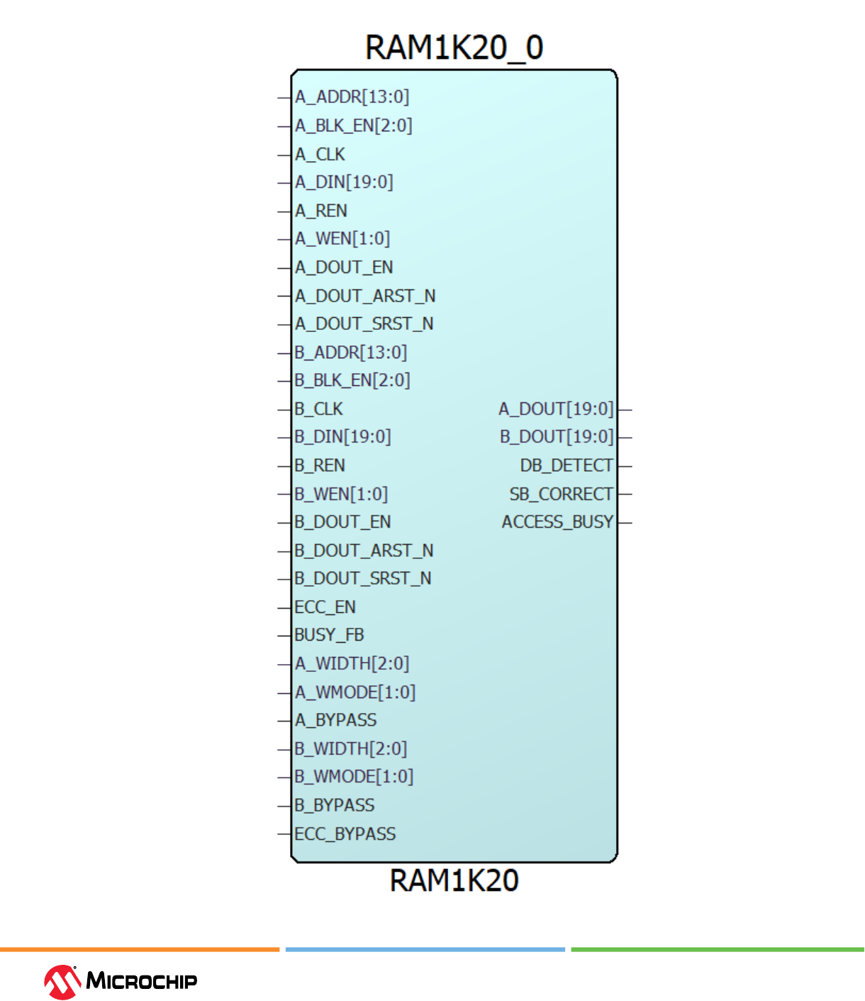
Appendix: Macro Conguraon
User Guide
© 2023 Microchip Technology Inc. and its subsidiaries
DS60001725G - 89
Figure 5-1. RAM1K20 Macro
Appendix: Macro Conguraon
User Guide
© 2023 Microchip Technology Inc. and its subsidiaries
DS60001725G - 90
The following table lists the ports of RAM1K20.
Table 5-1. Port List of RAM1K20
Pin Name Direction Type
1
Polarity Description
A_ADDR[13:0] Input Dynamic — Port A address
BLK_EN[2:0] Input Dynamic Active High Port A block selects
A_CLK Input Dynamic Rising edge Port A clock
A_DIN[19:0] Input Dynamic — Port A write data
A_DOUT[19:0] Output Dynamic — Port A read data
A_WEN[1:0] Input Dynamic Active High Port A write-enables (per byte)
A_REN Input Dynamic Active High Port A read-enable
A_WIDTH[2:0] Input Static — Port A width/depth mode select
A_WMODE[1:0] Input Static Active High Port A read-before-write and feed-through write selects
A_BYPASS Input Static Active High Port A pipeline register bypassed when High
A_DOUT_EN Input Dynamic Active High Port A pipeline register enable
A_DOUT_SRST_N Input Dynamic Active Low Port A pipeline register synchronous reset
A_DOUT_ARST_N Input Dynamic Active Low Port A pipeline register asynchronous reset
B_ADDR[13:0] Input Dynamic — Port B address
B_BLK_EN[2:0] Input Dynamic Active High Port B block selects
B_CLK Input Dynamic Rising edge Port B clock
B_DIN[19:0] Input Dynamic — Port B write data
B_DOUT[19:0] Output Dynamic — Port B read data
B_WEN[1:0] Input Dynamic Active High Port B write-enables (per byte)
B_REN Input Dynamic Active High Port B read-enable
B_WIDTH[2:0] Input Static Mode select Port B width/depth mode select
B_WMODE[1:0] Input Static Active High Port B read-before-write and feed-through write selects
B_BYPASS Input Static Active High Port B pipeline register bypassed when High
B_DOUT_EN Input Dynamic Active High Port B pipeline register enable
B_DOUT_SRST_N Input Dynamic Active Low Port B pipeline register synchronous-reset
B_DOUT_ARST_N Input Dynamic Active Low Port B pipeline register asynchronous-reset
ECC_EN Input Static Active High Enable ECC
ECC_BYPASS Input Static Active High ECC pipeline register bypassed when High
SB_CORRECT Output Dynamic Active High Single-bit correct ag
DB_DETECT Output Dynamic Active High Double-bit detect ag
BUSY_FB Input Static Active High Lock access to SmartDebug
ACCESS_BUSY Output Dynamic Active High Busy signal when being initialized or accessed using
SmartDebug
Note:
1. Static inputs are dened at design time and need to be tied to 0 or 1.
5.1.1 A_WIDTH and B_WIDTH (Ask a Queson)
Two-port mode is in eect when the width of at least one port is greater than 20 bits, and A_WIDTH
indicates the read width while B_WIDTH indicates the write width. The following table lists the width/
depth mode selections for each port.
Table 5-2. Width/Depth Mode Selecon
Depth x Width A_WIDTH/B_WIDTH
16K x 1 000
Appendix: Macro Conguraon
User Guide
© 2023 Microchip Technology Inc. and its subsidiaries
DS60001725G - 91
...........continued
Depth x Width A_WIDTH/B_WIDTH
8K x 2 001
4K x 4, 4K x 5 010
2K x 8, 2K x 10 011
1K x 16, 1K x 20 100
512 x 32 (two-port)
512 x 40 (two-port)
512 x 33 (two-port ECC)
101
5.1.2 A_WEN and B_WEN (Ask a Queson)
Two-port mode is in eect when the width of at least one port is greater than 20 bits, and read
operation is always enabled. The following table lists the write/read control signals for each port.
Table 5-3. Write/Read Operaon Select
Depth x Width A_WEN/B_WEN Result
16K x 1, 8K x 2, 4K x 5, 2K x 10 x0 Perform a read operation
16K x 1, 8K x 2, 4K x 5, 2K x 10 x1 Perform a write operation
1K x 16 00 Perform a read operation
01 Write [8:5], [3:0]
10 Write [18:15], [13:10]
11 Write [18:15], [13:10], [8:5], [3:0]
1K x 20 00 Perform a read operation
01 Write [9:0]
10 Write [19:10]
11 Write [19:0]
512 x 32 (two-port write) B_WEN[0] = 1 Write B_DIN[8:5], B_DIN[3:0]
B_WEN[1] = 1 Write B_DIN[18:15], B_DIN[13:10]
A_WEN[0] = 1 Write A_DIN[8:5], A_DIN[3:0]
A_WEN[1] = 1 Write A_DIN[18:15], A_DIN[13:10]
512 x 40 (two-port write) B_WEN[0] = 1 Write B_DIN[9:0]
B_WEN[1] = 1 Write B_DIN[19:10]
A_WEN[0] = 1 Write A_DIN[9:0]
A_WEN[1] = 1 Write A_DIN[19:10]
512 x 33 (two-port ECC) B_WEN[1:0] = 11
A_WEN[1:0] = 11
Write B_DIN[16:0]
Write A_DIN[15:0]
5.1.3 A_ADDR and B_ADDR (Ask a Queson)
14 bits are required to address the 16K independent locations in x1 mode. In wider modes, fewer
address bits are used. The required bits are MSb justied and unused LSb bits must be tied to 0.
A_ADDR is synchronized by A_CLK, while B_ADDR is synchronized to B_CLK. Two-port mode is in
eect when the width of at least one port is greater than 20, and A_ADDR provides the read-address
while B_ADDR provides the write-address. The following table lists the address buses for the two
ports.
Table 5-4. Write/Read Operaon Select
Depth x Width A_ADDR/B_ADDR
Used Bits Unused Bits
(Must be Tied to 0)
16K x 1 [13:0] None

Appendix: Macro Conguraon
User Guide
© 2023 Microchip Technology Inc. and its subsidiaries
DS60001725G - 92
...........continued
Depth x Width A_ADDR/B_ADDR
Used Bits Unused Bits
(Must be Tied to 0)
8K x 2 [13:1] [0]
4K x 4, 4K x 5 [13:2] [1:0]
2K x 8, 2K x 10 [13:3] [2:0]
1K x 16, 1K x 20 [13:4] [3:0]
512 x 32 (two-port)
512 x 40 (two-port)
512 x 33 (two-port ECC)
[13:5] [4:0]
5.1.4 A_DIN and B_DIN (Ask a Queson)
The required bits are LSb justied and unused MSb bits must be tied to 0. Two-port mode is in
eect when the width of at least one port is greater than 20 bits, and A_DIN provides the MSb of
the write-data while B_DIN provides the LSb of the write-data. The following table lists the data input
buses for the two ports.
Table 5-5. Data Input Buses Used and Unused Bits
Depth x Width A_DIN/B_DIN
Used Bits Unused Bits
(Must be tied to 0)
16K x 1 [0] [19:1]
8K x 2 [1:0] [19:2]
4K x 4 [3:0] [19:4]
4K x 5 [4:0] [19:5]
2K x 8 [8:5] => [7:4],
[3:0] => [3:0]
[19:9],
[4]
2K x 10 [9:0] [19:10]
1K x 16 [18:15] => [15:12]
[13:10] => [11:8]
[8:5] => [7:4]
[3:0] => [3:0]
[19]
[14]
[9]
[4]
1K x 20 [19:0] None
512 x 32 (two-port write) A_DIN[18:15] => [31:28]
A_DIN[13:10] => [27:24]
A_DIN[8:5] => [23:20]
A_DIN[3:0] => [19:16]
B_DIN[18:15] => [15:12]
B_DIN[13:10] =>[11:8]
B_DIN[8:5] => [7:4]
B_DIN[3:0] => [3:0]
A_DIN[19]
A_DIN[14]
A_DIN[9]
A_DIN[4]
B_DIN[19]
B_DIN[14]
B_DIN[9]
B_DIN[4]
512 x 40 (two-port write) A_DIN[19:0] => [39:20] B_DIN[19:0] =>
[19:0]
None
512 x 33 (two-port ECC) A_DIN[15:0] => [32:17]
B_DIN[16:0] => [16:0]
A_DIN[19:16]
B_DIN[19:17]
5.1.5 A_DOUT and B_DOUT (Ask a Queson)
The required bits are LSb-justied. Two-port mode is in eect when the width of at least one port is
greater than 20, and A_DOUT provides the MSb of the read-data while B_DOUT provides the LSb of
the read-data. The following table lists the data output buses for the two ports.

Appendix: Macro Conguraon
User Guide
© 2023 Microchip Technology Inc. and its subsidiaries
DS60001725G - 93
Table 5-6. Data Output Buses Used and Unused Bits
Depth x Width A_ADDR/B_ADDR
Used Bits Unused Bits
(must be tied to 0)
16K x 1 [0] [19:1]
8K x 2 [1:0] [19:2]
4K x 4 [3:0] [19:4]
4K x 5 [4:0] [19:5]
2K x 8 [8:5] => [7:4]
[3:0] => [3:0]
[19:9]
[4]
2K x 10 [9:0] [19:10]
1K x 16 [18:15] => [15:12]
[13:10] => [11:8]
[8:5] => [7:4]
[3:0] => [3:0]
[19]
[14]
[9]
[4]
1K x 20 [19:0] None
512 x 32 (two-port write) A_DIN[18:15] => [31:28]
A_DIN[13:10] => [27:24]
A_DIN[8:5] => [23:20]
A_DIN[3:0] => [19:16]
B_DIN[18:15] => [15:12]
B_DIN[13:10] => [11:8]
B_DIN[8:5] => [7:4]
B_DIN[3:0] => [3:0]
A_DIN[19]
A_DIN[14]
A_DIN[9]
A_DIN[4]
B_DIN[19]
B_DIN[14]
B_DIN[9]
B_DIN[4]
512 x 40 (two-port write) A_DOUT[19:0] => [39:20] B_DOUT[19:0] =>
[19:0]
None
512 x 33 (two-port ECC) A_DOUT[15:0] => [32:17] B_DOUT[16:0] =>
[16:0]
A_DOUT[19:16]
B_DOUT[19:17]
5.1.6 A_BLK_EN and B_BLK_EN (Ask a Queson)
A_BLK_EN is synchronized to A_CLK, while B_BLK_EN is synchronized to B_CLK. When two-port mode
is in eect, the width of at least one port is greater than 20 bits, A_BLK_EN controls the read
operation, and B_BLK_EN controls the write operation. The following table lists the block-port select
control signals for the two ports.
Table 5-7. Block-Port Select
Block-Port
Select Signal
Value Result
A_BLK_EN[2:0] 111 Perform read or write operation on Port A. If the width is greater than 20 bits, a
read is performed from both ports A and B.
A_BLK_EN[2:0] Any one bit is 0 No operation in memory from Port A. Port A read data is forced to 0. If the width is
greater than 20 bits, the read-data from both ports A and B is forced to 0.
B_BLK_EN[2:0] 111 Perform read or write operation on Port B, unless the width is greater than 20 bits
and a write is performed to both ports A and B.
B_BLK_EN[2:0] Any one bit is 0 No operation in memory from Port B. Port B read data is forced to 0, unless the
width is greater than 20 bits and write operation to both ports A and B is gated.
5.1.7 A_WMODE and B_WMODE (Ask a Queson)
In Dual-Port write mode, each port has a feed-through write or read-before-write option. When
A_WMODE or B_WMODE is equal to:
• Logic 00 = Simple Write. Read-data port holds the previous value.
Appendix: Macro Conguraon
User Guide
© 2023 Microchip Technology Inc. and its subsidiaries
DS60001725G - 94
• Logic 01 = Feed-through. Write-data appears on the corresponding read-data port. This setting is
invalid when the width of at least one port is greater than 20 bits and the two-port mode is in
eect.
• Logic 10 = Read-before-write. The previous content of the memory appears on the corresponding
read-data port before it is overwritten. This setting is invalid when the width of at least one port is
greater than 20 bits and the two-port mode is in eect.
5.1.8 A_CLK and B_CLK (Ask a Queson)
All signals in ports A and B are synchronous to the corresponding port clock. All addresses, data,
block-port select, write-enable, and read-enable inputs must be set up before the rising edge of the
clock. The read or write operation begins with the rising edge. Two-port mode is in eect when the
width of at least one port is greater than 20 bits, and A_CLK provides the read clock while B_CLK
provides the write clock.
5.1.9 A_REN and B_REN (Ask a Queson)
Enables read operation from the memory on the corresponding port. Two-port read mode is in
eect when the width of Port A is greater than 20 bits, and A_REN controls the read operation.
5.1.9.1 Read-Data Pipeline Register Control Signals (Ask a Queson)
• A_BYPASS and B_BYPASS
• A_DOUT_EN and B_DOUT_EN
• A_DOUT_SRST_N and B_DOUT_SRST_N
• A_DOUT_ARST_N and B_DOUT_ARST_N
Two-port mode is in eect when the width of at least one port is greater than 20 bits, and the
A_DOUT register signals control the MSb of the read-data, while the B_DOUT register signals control
the LSb of the read-data.
The following table lists the functionality of the control signals on the A_DOUT and B_DOUT pipeline
registers.
Table 5-8. Truth Table for A_DOUT and B_DOUT Registers
ARST_N A_BYPASS/
B_BYPASS
A_CLK/B_CLK A_EN/B_EN A_SRST_N/
B_SRST_N
D Qn+1
0 X X X X X 0
1 0 Not rising X X X Qn
1 0 ↑ 0 X X Qn
1 0 ↑ 1 0 X 0
1 0 ↑ 1 1 D D
1 1 X X X D D
5.1.10 ECC_EN and ECC_BYPASS (Ask a Queson)
The ECC operation is only allowed in two-port mode when the width of both ports is greater than 20
bits.
• ECC_EN = 0—disable ECC.
• ECC_EN = 1, ECC_BYPASS= 0—enable ECC Pipelined.
– ECC Pipelined mode inserts an additional clock cycle to read-data. In addition, write-feed-
through, and read-before-write modes add another clock cycle to read-data.
• ECC_EN = 1, ECC_BYPASS= 1—enable ECC Non-pipelined.

Appendix: Macro Conguraon
User Guide
© 2023 Microchip Technology Inc. and its subsidiaries
DS60001725G - 95
5.1.11 SB_CORRECT and DB_DETECT (Ask a Queson)
ECC ags become available when the ECC operation is enabled in two-port mode and the width of
both ports is greater than 20. The following table lists the functionality of the error detection and
correction ags.
Table 5-9. Error Detecon and Correcon Flags
DB_DETECT SB_CORRECT Flag
0 0 No errors detected
0 1 A single bit error is detected and corrected in the data output.
1 1 Multiple bit errors are detected, but are not corrected.
5.1.12 BUSY_FB (Ask a Queson)
When the control signal is set to 1, the entire RAM1K20 memory is locked o from being accessed by
the SmartDebug.
5.1.13 ACCESS_BUSY (Ask a Queson)
This output indicates that the RAM1K20 memory is being accessed by SmartDebug.
5.2 μSRAM Macro (Ask a Queson)
The μSRAM macro (RAM64x12) in Libero SoC can be used directly to instantiate μSRAM in the design.
μSRAM must be congured correctly with appropriate values provided to the static signals before
instantiating in the design. Instantiating μSRAM primitives in a design is not recommended. For the
recommended methods of instantiating memory into a user design, see 2.2.4.3. μSRAM Memory
Macro. The following gure shows the μSRAM macro (RAM64x12) available in the Libero SoC macro
library.
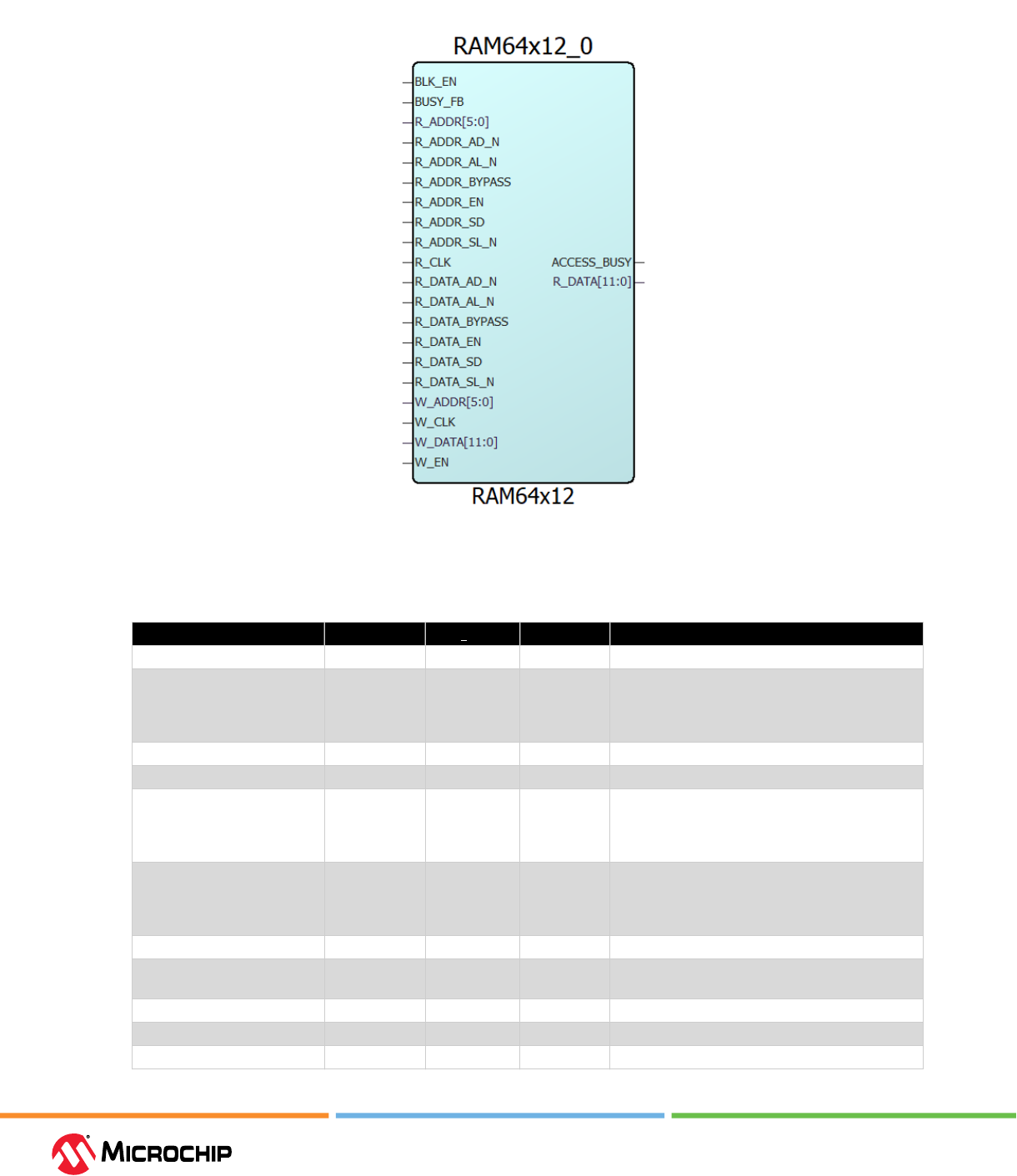
Appendix: Macro Conguraon
User Guide
© 2023 Microchip Technology Inc. and its subsidiaries
DS60001725G - 96
Figure 5-2. RAM64x12 Macro
The following table lists the ports of RAM64x12.
Table 5-10. Port List for RAM64x12
Pin Name Direction Type
1
Polarity Description
W_EN Input Dynamic Active high Write port enable
W_CLK Input Dynamic Rising edge Write clock. All write-address, write-data, and
write-enable inputs must be set up before the
rising edge of the clock. The write operation
begins with the rising edge.
W_ADDR[5:0] Input Dynamic — Write address
W_DATA[11:0] Input Dynamic Write-data
BLK_EN Input Dynamic Active high Read port block select. When High, a read
operation is performed. When Low, read-data
is forced to zero. BLK_EN signal is registered
through R_CLK when R_ADDR_BYPASS is Low.
R_CLK Input Dynamic Rising edge Read registers clock. All read-address, block-port
select, and read-enable inputs must be set up
before the rising edge of the clock. The read
operation begins with the rising edge.
R_ADDR[] Input Dynamic Read-address
R_ADDR_BYPASS Input Static Active high Read-address and BLK_EN register bypassed
when high
R_ADDR_EN Input Dynamic Active high Read-address register enable
R_ADDR_SL_N Input Dynamic Active low Read-address register synchronous load
R_ADDR_SD Input Static Active high Read-address register synchronous load data
Appendix: Macro Conguraon
User Guide
© 2023 Microchip Technology Inc. and its subsidiaries
DS60001725G - 97
...........continued
Pin Name Direction Type
1
Polarity Description
R_ADDR_AL_N Input Dynamic Active low Read-address register asynchronous load
R_ADDR_AD_N Input Static Active low Read-address register asynchronous load data
R_DATA[] Output Dynamic Read-data
R_DATA_BYPASS Input Static Active high Read-data pipeline register bypassed when high
R_DATA_EN Input Dynamic Active high Read-data pipeline register enable
R_DATA_SL_N Input Dynamic Active low Read-data pipeline register synchronous load
R_DATA_SD Input Static Active high Read-data pipeline register synchronous load
data
R_DATA_AL_N Input Dynamic Active low Read-data pipeline register asynchronous load
R_DATA_AD_N Input Static Active low Read-data pipeline register asynchronous load
data
BUSY_FB Input Static Active high Lock access to SmartDebug
ACCESS_BUSY Output Dynamic Active high Busy signal from SmartDebug
Note:
(1)
Static inputs are dened at design time and need to be tied to 0 or 1.
5.2.1 Read-Address and Read-Data Pipeline Register Control Signals (Ask a Queson)
The following table lists the functionality of the control signals on the R_ADDR and R_DATA registers.
Table 5-11. Truth Table for A_DOUT and B_DOUT Registers
A_AL_N/
B_AL_N
A_AD_N/
B_AD_N
A_BYPASS/
B_BYPASS
A_CLK/
B_CLK
A_EN/
B_EN
A_SL_N/
B_SL_N
A_SD/
B_SD
D Qn+1
0 ADn X X X X X X !ADn
1 X 0 Not rising X X X X Qn
1 X 0 ↑ 0 X X X Qn
1 X 0 ↑ 1 0 SD X SD
1 X 0 ↑ 1 1 X D D
1 X 1 X X X X D D
5.3 Math Block Macro (Ask a Queson)
Two math block macros, MACC_PA and MACC_PA_BC_ROM, are available in Libero SoC IP catalog
macro library. These macros can be used in designs created with SmartDesign or by directly
instantiating the macro wrapper in an HDL le as a component. Instantiating math block primitives
in a design is not recommended. For the recommended methods of instantiating math blocks into
a user design, see 3.6. Implementation. When using the macros, the inputs and outputs must
be connected manually to the design signals. Proper values for the static signals must also be
provided to ensure that the math block is congured in the correct operational mode. For example,
to congure the math block in DOTP mode, the DOTP signal must be tied to logic 1.
5.3.1 MACC_PA (MACC with Pre-Adder) (Ask a Queson)
The MACC_PA is the multiply and accumulator with pre-adder macro block. The MACC_PA macro
implements multiplication, multiply-add, and multiply-accumulate functions. The MACC_PA block can
accumulate the current multiplication product with a previous result, a constant, a dynamic value,
or a result from another MACC_PA block. Each MACC_PA block can also be congured to perform a
DOTP operation. All the signals of the MACC_PA block have optional registers.
The following gure shows the MACC_PA available in the macro library.
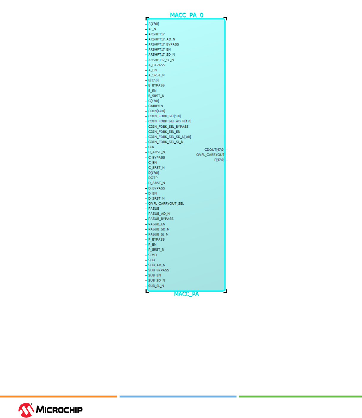

Appendix: Macro Conguraon
User Guide
© 2023 Microchip Technology Inc. and its subsidiaries
DS60001725G - 99
Table 5-12. MACC_PA Pin Descripons
Port Name Direction Type
1
Polarity Description
DOTP Input Static Active high DOTP mode
When DOTP = 1, MACC_PA block performs DOTP of
two pairs of 9-bit operands.
• SIMD must not be 1
• C[8:0] must be connected to CARRYIN.
SIMD Input Static Active high SIMD mode
When SIMD = 1, MACC_PA block performs dual-
independent multiplication of two pairs of 9-bit
operands.
DOTP must not be 1
ARSHFT17 must be 0
D[8:0] must be 0
C[17:0] must be 0
E[17:0] must be 0. For more information about how
operand E is obtained from P, CDIN, or 0, see Table
3-3.
OVFL_CARRYOUT_SEL Input Static Active high Generate OVERFLOW or CARRYOUT with result
P. OVERFLOW when OVFL_CARRYOUT_SEL = 0
CARRYOUT when OVFL_CARRYOUT_SEL = 1
CLK Input Dynamic Rising edge Clock for A, B, C, CARRYIN, D, P, OVFL_CARRYOUT,
ARSHFT17, CDIN_FDBK_SEL, PASUB, and SUB
registers.
AL_N Input Dynamic Active low Asynchronous load for A, B, P, OVFL_CARRYOUT,
ARSHFT17, CDIN_FDBK_SEL, PASUB, and SUB
registers. Connect to 1 if not registered.
When asserted, A, B, P, and OVFL_CARRYOUT
registers are loaded with zero, while the ARSHFT17,
CDIN_FDBK_SEL, PASUB, and SUB registers are
loaded with the complementary value of the
respective _AD_N.
A[17:0] Input Dynamic Active high Input data A
A_BYPASS Input Static Active high Bypass data A registers. Connect to 1 if not
registered. For more information, see Table 5-14.
A_SRST_N Input Dynamic Active low Synchronous reset for data A registers. Connect to
1 if not registered. For more information, see Table
5-14.
A_EN Input Dynamic Active high Enable for data A registers. Connect to 1 if not
registered. For more information, see Table 5-14.
B[17:0] Input Dynamic Active high Input data B to pre-adder with data D.
B_BYPASS Input Static Active high Bypass data B registers. Connect to 1 if not
registered. For more information, see Table 5-14.
B_SRST_N Input Dynamic Active low Synchronous reset for data B registers. Connect to
1 if not registered. For more information, see Table
5-14.
B_EN Input Dynamic Active high Enable for data B registers. Connect to 1 if not
registered. For more information, see Table 5-14.
D[17:0] Input Dynamic Active high Input data D to pre-adder with data B.
When SIMD = 1, connect D[8:0] to 0.

Appendix: Macro Conguraon
User Guide
© 2023 Microchip Technology Inc. and its subsidiaries
DS60001725G - 100
...........continued
Port Name Direction Type
1
Polarity Description
D_BYPASS Input Static Active high Bypass data D registers. Connect to 1 if not
registered. For more information, see Table 5-15.
D_ARST_N Input Dynamic Active low Asynchronous reset for data D registers. Connect to
1 if not registered. For more information, see Table
5-15.
D_SRST_N Input Dynamic Active low Synchronous reset for data D registers. Connect to
1 if not registered. For more information, see Table
5-15.
D_EN Input Dynamic Active high Enable for data D registers. Connect to 1 if not
registered. For more information, see Table 5-15.
CARRYIN Input Dynamic Active high CARRYIN for input data C.
C[47:0] Input Dynamic Active high Input data C.
When DOTP = 1, connect C[8:0] to CARRYIN.
When SIMD = 1, connect C[8:0] to 0.
C_BYPASS Input Static Active high Bypass CARRYIN and C registers. Connect to 1 if not
registered. For more information, see Table 5-15.
C_ARST_N Input Dynamic Active low Asynchronous reset for CARRYIN and C registers.
Connect to 1 if not registered. For more information,
see Table 5-15.
C_SRST_N Input Dynamic Active low Synchronous reset for CARRYIN and C registers.
Connect to 1 if not registered. For more information,
see Table 5-15.
C_EN Input Dynamic Active high Enable for CARRYIN and C registers. Connect to 1
if not registered. For more information, see Table
5-15.
CDIN[47:0] Input Cascade Active high Cascaded input for operand E.
The entire bus must be driven by an entire
CDOUT of another MACC_PA or MACC_PA_BC_ROM
block. In DOTP mode, the driving CDOUT must also
be generated by a MACC_PA or MACC_PA_BC_ROM
block in DOTP mode. For more information about
how CDIN is propagated to operand E, see Table 3-3.
P[47:0] Output Active high Result data. For more information, see Table 3-4.
OVFL_CARRYOUT Output Active high OVERFLOW or CARRYOUT. For more information,
see Table 3-4.
P_BYPASS Input Static Active high Bypass P and OVFL_CARRYOUT registers. Connect to
1 if not registered. For more information, see Table
5-14.
P_SRST_N Input Dynamic Active low Synchronous reset for P and OVFL_CARRYOUT
registers. Connect to 1 if not registered. For more
information, see Table 5-14.
P_EN Input Dynamic Active high Enable for P and OVFL_CARRYOUT registers.
Connect to 1 if not registered. For more information,
see Table 5-14.

Appendix: Macro Conguraon
User Guide
© 2023 Microchip Technology Inc. and its subsidiaries
DS60001725G - 101
...........continued
Port Name Direction Type
1
Polarity Description
CDOUT[47:0] Output Cascade Active high Cascade output of result P. For more information,
see Table 3-4.
Value of CDOUT is the same as P. The entire bus
must either be dangling or drive an entire CDIN
of another MACC_PA or MACC_PA_BC_ROM block in
cascaded mode.
PASUB Input Dynamic Active high Subtract operation for pre-adder of B and D.
PASUB_BYPASS Input Static Active high Bypass PASUB register. Connect to 1 if not
registered. For more information, see Table 5-13.
PASUB_AD_N Input Static Active low Asynchronous load data for PASUB register. For
more information, see Table 5-13.
PASUB_SL_N Input Dynamic Active low Synchronous load for PASUB register. Connect to 1
if not registered. For more information, see Table
5-13.
PASUB_SD_N Input Static Active low Synchronous load data for PASUB register. For more
information, see Table 5-13.
PASUB_EN Input Dynamic Active high Enable for PASUB register. Connect to 1 if not
registered. For more information, see Table 5-13.
CDIN_FDBK_SEL[1:0] Input Dynamic Active high Select CDIN, P or 0 for operand E. For more
information, see Table 3-3.
CDIN_FDBK_SEL_BYPASS Input Static Active high Bypass CDIN_FDBK_SEL register. Connect to 1 if not
registered. For more information, see Table 5-13.
CDIN_FDBK_SEL_AD_N
[1:0]
Input Static Active low Asynchronous load data for CDIN_FDBK_SEL
register. For more information, see Table 5-13.
CDIN_FDBK_SEL_SL_N Input Dynamic Active low Synchronous load for CDIN_FDBK_SEL register.
Connect to 1 if not registered. For more information,
see Table 5-13.
CDIN_FDBK_SEL_SD_N
[1:0]
Input Static Active low Synchronous load data for CDIN_FDBK_SEL register.
For more information, see Table 5-13.
CDIN_FDBK_SEL_EN Input Dynamic Active high Enable for CDIN_FDBK_SEL register. Connect to 1
if not registered. For more information, see Table
5-13.
ARSHFT17 Input Dynamic Active high Arithmetic right-shift for operand E.
When asserted, a 17-bit arithmetic right-shift is
performed on operand E. For information on how
operand E is obtained from P, CDIN or 0, see Table
3-3.
When SIMD = 1, ARSHFT17 must be 0.
ARSHFT17_BYPASS Input Static Active high Bypass ARSHFT17 register. Connect to 1 if not
registered. For more information, see Table 5-13.
ARSHFT17_AD_N Input Static Active low Asynchronous load data for ARSHFT17 register. For
more information, see Table 5-13.
ARSHFT17_SL_N Input Dynamic Active low Synchronous load for ARSHFT17 register. Connect to
1 if not registered. For more information, see Table
5-13.
ARSHFT17_SD_N Input Static Active low Synchronous load data for ARSHFT17 register. For
more information, see Table 5-13.
ARSHFT17_EN Input Dynamic Active high Enable for ARSHFT17 register. Connect to 1 if not
registered. For more information, see Table 5-13.
SUB Input Dynamic Active high Subtract operation.
Appendix: Macro Conguraon
User Guide
© 2023 Microchip Technology Inc. and its subsidiaries
DS60001725G - 102
...........continued
Port Name Direction Type
1
Polarity Description
SUB_BYPASS Input Static Active high Bypass SUB register. Connect to 1 if not registered.
For more information, see Table 5-13.
SUB_AD_N Input Static Active low Asynchronous load data for SUB register. For more
information, see Table 5-13.
SUB_SL_N Input Dynamic Active low Synchronous load for SUB register. Connect to 1
if not registered. For more information, see Table
5-13.
SUB_SD_N Input Static Active low Synchronous load data for SUB register. For more
information, see Table 5-13.
SUB_EN Input Dynamic Active high Enable for SUB register. Connect to 1 if not
registered. For more information, see Table 5-13.
Note:
(1)
Static inputs are dened at design time and need to be tied to 0 or 1.
Note: SUM[49:0] is dened similarly to P[47:0] as listed in Table 3-4, except that SUM is a 50-bit
quantity so that overow does not occur. SUM[48] is the carry out bit of a 48-bit nal adder that
produces P[47:0].
Table 5-13. Truth Table for Control Registers ARSHFT17, CDIN_FDBK_SEL, PASUB, and SUB
AL_N _AD_N _BYPASS CLK _EN _SL_N _SD_N D Qn+1
0 AD_N 0 X X X X X !AD_N
1 X 0 Not rising X X X X Qn
1 X 0 ↑ 0 X X X Qn
1 X 0 ↑ 1 0 SD_N X !SD_N
1 X 0 ↑ 1 1 X D D
X X 1 X 0 X X X Qn
X X 1 X 1 0 SD_N X !SD_N
X X 1 X 1 1 X D D
Table 5-14. Truth Table for Data Registers A, B, P, and OVFL_CARRYOUT
AL_N _BYPASS CLK _EN _SRST_N D Qn+1
0 0 X X X X 0
1 0 Not rising X X X Qn
1 0 ↑ 0 X X Qn
1 0 ↑ 1 0 X 0
1 0 ↑ 1 1 D D
X 1 X 0 X X Qn
X 1 X 1 0 X 0
X 1 X 1 1 D D
Table 5-15. Truth Table for Data Registers C, CARRYIN, and D
_ARST_N _BYPASS CLK _EN _SRST_N D Qn+1
0 0 X X X X 0
1 0 Not rising X X X Qn
1 0 ↑ 0 X X Qn
1 0 ↑ 1 0 X 0
1 0 ↑ 1 1 D D
X 1 X 0 X X Qn

Appendix: Macro Conguraon
User Guide
© 2023 Microchip Technology Inc. and its subsidiaries
DS60001725G - 103
...........continued
_ARST_N _BYPASS CLK _EN _SRST_N D Qn+1
X 1 X 1 0 X 0
X 1 X 1 1 D D
5.3.2 MACC_PA_BC_ROM (MACC with Pre-Adder, BCOUT Register, and Coecient ROM) (Ask a
Queson)
The MACC_PA_ROM is the multiply accumulator with pre-adder, B register cascading, and built-in
ROM macro block. The MACC_PA_BC_ROM macro extends the functionality of the MACC_PA macro to
provide a 16 x 18 ROM at the A input along with a pipelined output of B for cascading.
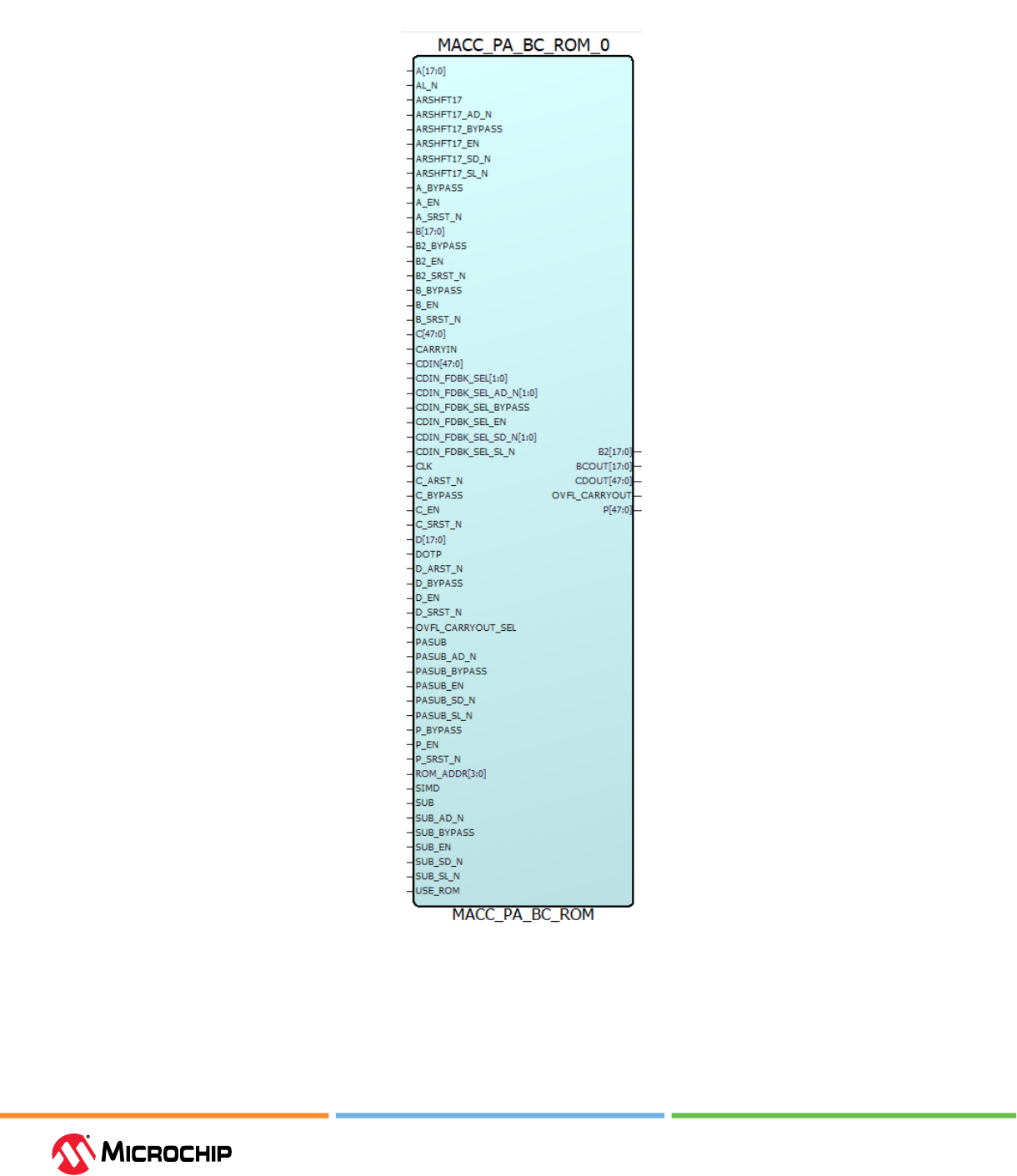
Appendix: Macro Conguraon
User Guide
© 2023 Microchip Technology Inc. and its subsidiaries
DS60001725G - 104
Figure 5-4. MACC_PA_BC_ROM Macro
5.3.2.1 Parameters (Ask a Queson)
Coecients are loaded using INIT parameter. It holds the 16 x 18 ROM content as a linear array.
The rst 18 bits are word 0, the next 18 bits are word 1, and so on. The following table lists the INIT
declaration for loading coecients.

Appendix: Macro Conguraon
User Guide
© 2023 Microchip Technology Inc. and its subsidiaries
DS60001725G - 105
Table 5-16. MACC_PA_BC_ROM Parameter Descripons
Parameter Dimensions Description
INIT parameter [287:0] INIT = {
18'h0, 18'h0, 18'h0, 18'h0, 18'h0, 18'h0, 18'h0, 18'h0,
18'h0, 18'h0, 18'h0, 18'h0, 18'h0, 18'h0, 18'h0, 18'h0
};
16 x 18 ROM content specied in
Verilog.
INIT generic map(INIT => (
B“00_0000_0000_0000_0000”& B“00_0000_0000_0000_0000”&
B“00_0000_0000_0000_0000”& B“00_0000_0000_0000_0000”&
B“00_0000_0000_0000_0000”& B“00_0000_0000_0000_0000”&
B“00_0000_0000_0000_0000”& B“00_0000_0000_0000_0000”&
B“00_0000_0000_0000_0000”& B“00_0000_0000_0000_0000”&
B“00_0000_0000_0000_0000”& B“00_0000_0000_0000_0000”&
B“00_0000_0000_0000_0000”& B“00_0000_0000_0000_0000”&
B“00_0000_0000_0000_0000”& B“00_0000_0000_0000_0000”)
)
16 x 18 ROM content specied in
VHDL.
5.3.2.2 Port List (Ask a Queson)
Table 5-17. MACC_PA_BC_ROM Pin Descripons
Port Name Direction Type
1
Polarity Description
DOTP Input Static Active high DOTP mode.
When DOTP = 1, MACC_PA_BC_ROM
block performs DOTP of two pairs of
9-bit operands.
SIMD must not be 1.
C[8:0] must be connected to CARRYIN.
SIMD Input Static Active high SIMD mode
When SIMD = 1, MACC_PA_BC_ROM
block performs dual independent
multiplication of two pairs of 9-bit
operands.
DOTP must not be 1
ARSHFT17 must be 0
D[8:0] must be 0
C[17:0] must be 0
E[17:0] must be 0. For information on
how operand E is obtained from P,
CDIN or 0, see Table 3-3.
OVFL_CARRYOUT_SEL Input Static Active high Generate OVERFLOW or CARRYOUT
with result P.
OVERFLOW when
OVFL_CARRYOUT_SEL = 0 CARRYOUT
when OVFL_CARRYOUT_SEL = 1
CLK Input Dynamic Rising edge Clock for A, B, C, CARRYIN,
D, P, OVFL_CARRYOUT, ARSHFT17,
CDIN_FDBK_SEL, PASUB, and SUB
registers.

Appendix: Macro Conguraon
User Guide
© 2023 Microchip Technology Inc. and its subsidiaries
DS60001725G - 106
...........continued
Port Name Direction Type
1
Polarity Description
AL_N Input Dynamic Active low Asynchronous load for A, B,
P, OVFL_CARRYOUT, ARSHFT17,
CDIN_FDBK_SEL, PASUB, and SUB
registers. Connect to 1, if none are
registered.
When asserted, A, B, P, and
OVFL_CARRYOUT registers are loaded
with zero, while the ARSHFT17,
CDIN_FDBK_SEL, PASUB, and SUB
registers are loaded with the
complementary value of the respective
_AD_N.
USE_ROM Input Static (virtual) Active high Selection for operand A.
When USE_ROM = 0, select input data
A.
When USE_ROM = 1, select ROM data
at ROM_ADDR.
ROM_ADDR[3:0] Input Dynamic Active high Address of ROM data for operand A
when USE_ROM = 1
A[17:0] Input Dynamic Active high Input data for operand A when
USE_ROM = 0
A_BYPASS Input Static Active high Bypass data A registers. Connect to 1
if not registered. For more information,
see Table 5-14.
A_SRST_N Input Dynamic Active low Synchronous reset for data A registers.
Connect to 1 if not registered. For
more information, see Table 5-14.
A_EN Input Dynamic Active high Enable for data A registers. Connect
to 1 if not registered. For more
information, see Table 5-14.
B[17:0] Input Dynamic Active high Input data B to pre-adder with data D
B_BYPASS Input Static Active high Bypass data B registers. Connect to 1
if not registered. For more information,
see Table 5-14.
B_SRST_N Input Dynamic Active low Synchronous reset for data B registers.
Connect to 1 if not registered. For
more information, see Table 5-14.
B_EN Input Dynamic Active high Enable for data B registers. Connect
to 1 if not registered. For more
information, see Table 5-14.
B2[17:0] Output Dynamic Active high Pipelined output of input data B. Result
P must be oating when B2 is used.
B2_BYPASS Input Static Active high Bypass data B2 registers. Connect to 1
if not registered. For more information,
see Table 5-14.
B2_SRST_N Input Dynamic Active low Synchronous reset for data B2
registers. Connect to 1 if not
registered. For more information, see
Table 5-14.
B2_EN Input Dynamic Active high Enable for data B2 registers. Connect
to 1 if not registered. For more
information, see Table 5-14.

Appendix: Macro Conguraon
User Guide
© 2023 Microchip Technology Inc. and its subsidiaries
DS60001725G - 107
...........continued
Port Name Direction Type
1
Polarity Description
BCOUT[17:0] Output Cascade Active high Cascade output of B2. Value of BCOUT
is the same as B2. The entire bus
must either be dangling or drive an
entire B input of another MACC_PA or
MACC_PA_BC_ROM block.
D[17:0] Input Dynamic Active high Input data D to pre-adder with data B.
When SIMD = 1, connect D[8:0] to 0.
D_BYPASS Input Static Active high Bypass data D registers. Connect to 1
if not registered. For more information,
see Table 5-15.
D_ARST_N Input Dynamic Active low Asynchronous reset for data D
registers. Connect to 1 if not
registered. For more information, see
Table 5-15.
D_SRST_N Input Dynamic Active low Synchronous reset for data D registers.
Connect to 1 if not registered. For
more information, see Table 5-15.
D_EN Input Dynamic Active high Enable for data D registers. Connect
to 1 if not registered. For more
information, see Table 5-15.
CARRYIN Input Dynamic Active high CARRYIN for input data C
C[47:0] Input Dynamic Active high Input data C.
When DOTP = 1, connect C[8:0] to
CARRYIN.
When SIMD = 1, connect C[8:0] to 0.
C_BYPASS Input Static Active high Bypass CARRYIN and C registers.
Connect to 1 if not registered. For
more information, see Table 5-15.
C_ARST_N Input Dynamic Active low Asynchronous reset for CARRYIN and
C registers. Connect to 1 if not
registered. For more information, see
Table 5-15.
C_SRST_N Input Dynamic Active low Synchronous reset for CARRYIN and
C registers. Connect to 1 if not
registered. For more information, see
Table 5-15.
C_EN Input Dynamic Active high Enable for CARRYIN and C registers.
Connect to 1 if not registered. For
more information, see Table 5-15.
CDIN[47:0] Input Cascade Active high Cascaded input for operand E.
The entire bus must be driven by an
entire
CDOUT of another MACC_PA or
MAC_PA_BC_ROM block. In Dot-
product mode, the driving CDOUT
must also be generated by a MACC_PA
or MAC_PA_BC_ROM block in Dot-
product mode. For more information
about how CDIN is propagated to
operand E, see Table 3-3.
P[47:0] Output — Active high Result data. For more information, see
Table 3-3. B2 output must be oating
when P is used.
OVFL_CARRYOUT Output — Active high OVERFLOW or CARRYOUT. For more
information, see Table 3-2.

Appendix: Macro Conguraon
User Guide
© 2023 Microchip Technology Inc. and its subsidiaries
DS60001725G - 108
...........continued
Port Name Direction Type
1
Polarity Description
P_BYPASS Input Static Active high Bypass P and OVFL_CARRYOUT
registers. Connect to 1 if not
registered. For more information, see
Table 5-14.
P_SRST_N Input Dynamic Active low Synchronous reset for P and
OVFL_CARRYOUT registers. Connect
to 1 if not registered. For more
information, see Table 5-14.
P_EN Input Dynamic Active high Enable for P and OVFL_CARRYOUT
registers. Connect to 1 if not
registered. For more information, see
Table 5-14.
CDOUT[47:0] Output Cascade Active high Cascade output of result P. For more
information, see Table 3-4.
Value of CDOUT is the same as P. The
entire bus must either be dangling
or drive an entire CDIN of another
MACC_PA or MAC_PA_BC_ROM block in
cascaded mode.
PASUB Input Dynamic Active high Subtract operation for pre-adder of B
and D
PASUB_BYPASS Input Static Active high Bypass PASUB register. Connect to 1 if
not registered. For more information,
see Table 5-13.
PASUB_AD_N Input Static Active low Asynchronous load data for PASUB
register. For more information, see
Table 5-13.
PASUB_SL_N Input Dynamic Active low Synchronous load for PASUB register.
Connect to 1 if not registered. For
more information, see Table 5-13.
PASUB_SD_N Input Static Active low Synchronous load data for PASUB
register. For more information, see
Table 5-13.
PASUB_EN Input Dynamic Active high Enable for PASUB register. Connect
to 1 if not registered. For more
information, see Table 5-13.
CDIN_FDBK_SEL[1:0] Input Dynamic Active high Select CDIN, P or 0 for operand E. For
more information, see Table 3-3.
CDIN_FDBK_SEL_BYPASS Input Static Active high Bypass CDIN_FDBK_SEL register.
Connect to 1 if not registered. For
more information, see Table 5-13.
CDIN_FDBK_SEL_AD_N [1:0] Input Static Active low Asynchronous load data for
CDIN_FDBK_SEL register. For more
information, see Table 5-13.
CDIN_FDBK_SEL_SL_N Input Dynamic Active low Synchronous load for CDIN_FDBK_SEL
register. Connect to 1 if not registered.
For more information, see Table 5-13.
CDIN_FDBK_SEL_SD_N [1:0] Input Static Active low Synchronous load data for
CDIN_FDBK_SEL register. For more
information, see Table 5-13.
CDIN_FDBK_SEL_EN Input Dynamic Active high Enable for CDIN_FDBK_SEL register.
Connect to 1 if not registered. For
more information, see Table 5-13.

Appendix: Macro Conguraon
User Guide
© 2023 Microchip Technology Inc. and its subsidiaries
DS60001725G - 109
...........continued
Port Name Direction Type
1
Polarity Description
ARSHFT17 Input Dynamic Active high Arithmetic right-shift for operand E.
When asserted, a 17-bit arithmetic
right-shift is performed on operand
E. For more information about how
operand E is obtained from P, CDIN or
0, see Table 3-3.
When SIMD = 1, ARSHFT17 must be 0.
ARSHFT17_BYPASS Input Static Active high Bypass ARSHFT17 register. Connect
to 1, if not registered. For more
information, see Table 5-13.
ARSHFT17_AD_N Input Static Active low Asynchronous load data for ARSHFT17
register. For more information, see
Table 5-13.
ARSHFT17_SL_N Input Dynamic Active low Synchronous load for ARSHFT17
register. Connect to 1 if not registered.
For more information, see Table 5-13.
ARSHFT17_SD_N Input Static Active low Synchronous load data for ARSHFT17
register. For more information, see
Table 5-13.
ARSHFT17_EN Input Dynamic Active high Enable for ARSHFT17 register. Connect
to 1 if not registered. For more
information, see Table 5-13.
SUB Input Dynamic Active high Subtract operation
SUB_BYPASS Input Static Active high Bypass SUB register. Connect to 1 if
not registered. For more information,
see Table 5-13.
SUB_AD_N Input Static Active low Asynchronous load data for SUB
register. For more information, see
Table 5-13.
SUB_SL_N Input Dynamic Active low Synchronous load for SUB register.
Connect to 1 if not registered. For
more information, see Table 5-13.
SUB_SD_N Input Static Active low Synchronous load data for SUB
register. For more information, see
Table 5-13.
SUB_EN Input Dynamic Active high Enable for SUB register. Connect to 1
if not registered. For more information,
see Table 5-13.
Note:
(1)
Static inputs are dened at design time and need to be tied to 0 or 1.
5.4 Libero SoC Compile Report (Ask a Queson)
Libero SoC Design Suite oers high productivity with its comprehensive, easy-to-learn, easy-to-adopt
development tools for designing with both the device families. The compile report contains fabric
resource utilization and the total number of resources available. This report provides the number
of 4LUTs, DFFs, μSRAMs, LSRAMs, math blocks, I/O, DLLs, PLLs, transceivers, and globals used in a
design. It also contains the additional 4LUTs and DFFs required for RAMs and MACC interface logic.
For a sample compile report on MPF300, see the following gure.
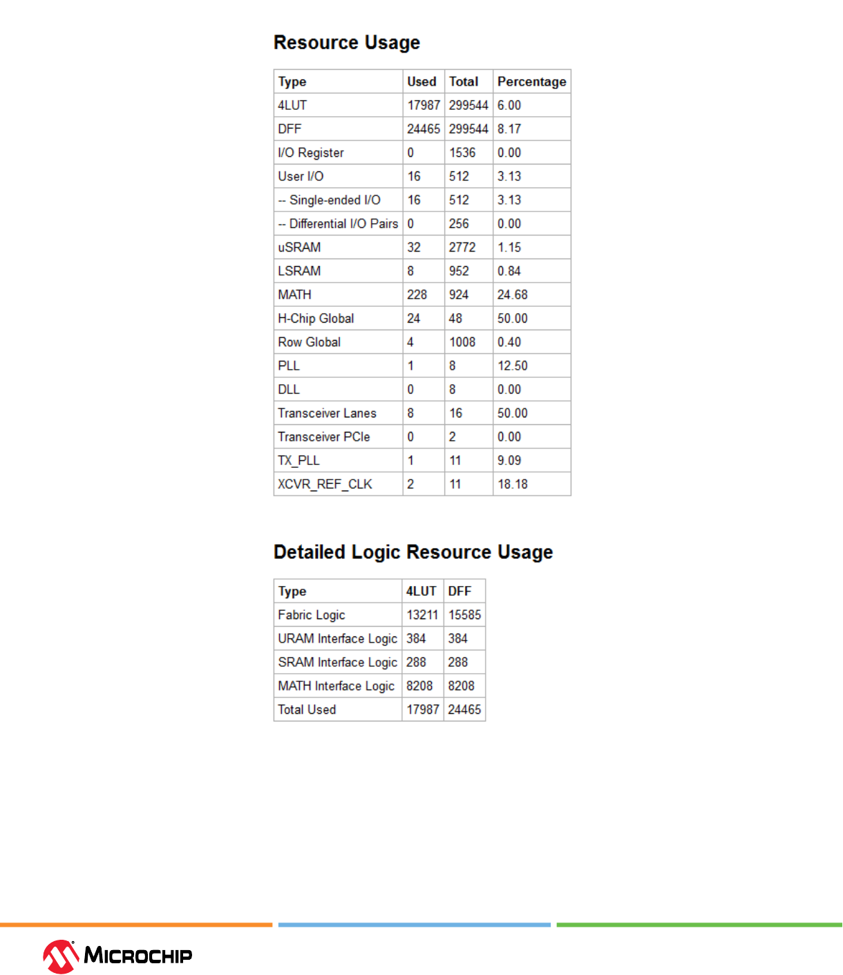
Appendix: Macro Conguraon
User Guide
© 2023 Microchip Technology Inc. and its subsidiaries
DS60001725G - 110
Figure 5-5. Sample Compile Report for MPF300
For a sample compile report on MPFS250, see the following gure.
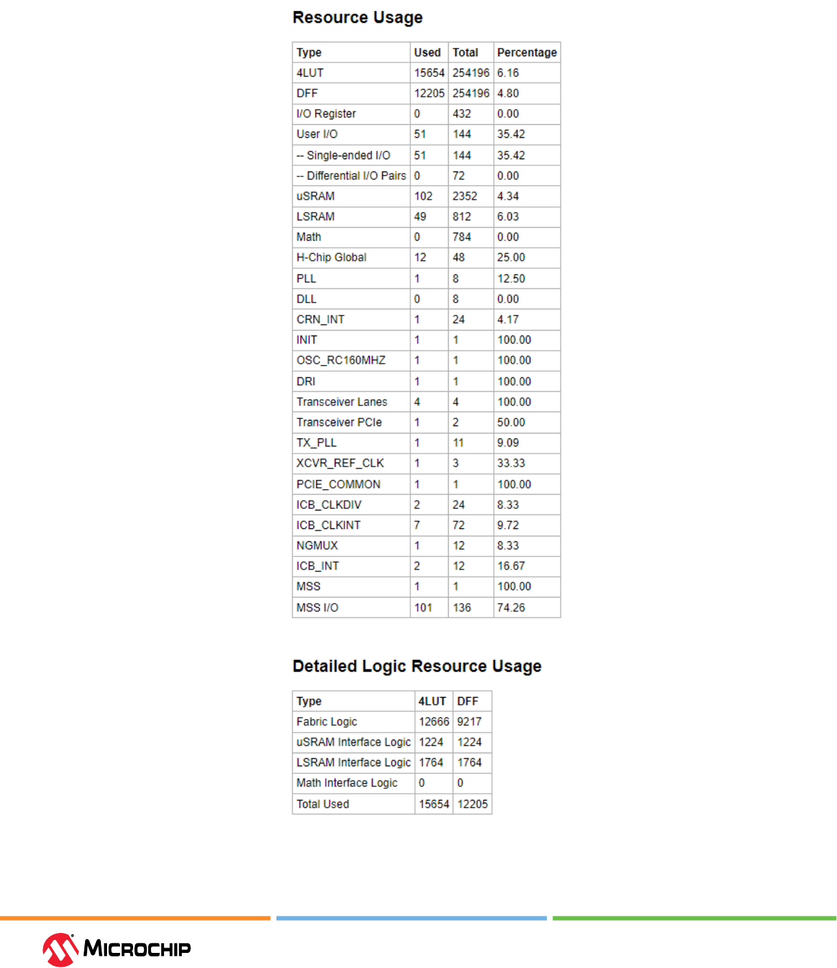
Appendix: Macro Conguraon
User Guide
© 2023 Microchip Technology Inc. and its subsidiaries
DS60001725G - 111
Figure 5-6. Sample Compile Report for MPFS250
For a sample compile report on RTPF500, see the following gure.

Appendix: Macro Conguraon
User Guide
© 2023 Microchip Technology Inc. and its subsidiaries
DS60001725G - 112
Figure 5-7. Sample Compile Report for RTPF500
To be updated.

References
User Guide
© 2023 Microchip Technology Inc. and its subsidiaries
DS60001725G - 113
6. References (Ask a Queson)
The following is the list of reference documents.
• For information about using Libero SoC for PolarFire and PolarFire SoC, see
Libero SoC Documentation.
• For information about the initialization of the fabric memory blocks during power-up, see
PolarFire Family Power-Up and Resets User Guide.
• For information about the security features in both product families, see PolarFire Family Security
User Guide.
• For information about the PolarFire SoC MSS, see PolarFire SoC FPGA MSS Technical Reference
Manual.

Revision History
User Guide
© 2023 Microchip Technology Inc. and its subsidiaries
DS60001725G - 114
7. Revision History (Ask a Queson)
The revision history table describes the changes that were implemented in the document. The
changes are listed by revision, starting with the most current publication.
Table 7-1. Revision History
Revision Date Description
G 09/2023 The following is the summary of changes in this revision of the
document:
• Added a line on how to enable the Reset All Values option
for RAM initialization. See 2.1.3.2.1. Dual-Port Large SRAM
Congurator, 2.1.3.2.2. Two-Port LSRAM Congurator, and
2.2.4.2.3. Memory Initialization at Power-Up.
• Updated the polarity and description of A_BYPASS, B_BYPASS,
and ECC_BYPASS signals in Table 2-2 and Table 5-1.
• Updated the polarity and description of R_ADDR_BYPASS and
R_DATA_BYPASS signals in Table 2-11 and Table 5-10.
F 03/2023 The following is the summary of changes in this revision of the
document:
• Updated the document title and added RT PolarFire information.
• In 2.3. μPROM, modied the sentence to mention that fabric
logic has read-only access to µPROM.
• Updated 2.1.2.5. ECC Mode (For x33 Two-Port Mode Only) to
include information about Multi-bit errors.
E 07/2022 The following is the summary of changes in this revision of the
document:
• Added the µPROM port BUSY, see Figure 2-28 and Table 2-13.
• Added sNVM storage space requirements for fabric RAM
initialization, see 2.4.1. Implementation
• Added 4. MEMFILE (RAM Content Manager output le)
D 03/2022 The following is the summary of changes in this revision of the
document:
• In 2.3.3.2.2. Content from File, added the supported memory
le formats
• Corrected the real value PX+QY to PX-QY in Figure 3-12
• Updated 2.1.3.2.1. Dual-Port Large SRAM Congurator and
2.1.3.2.2. Two-Port LSRAM Congurator for describing the
LSRAM behavior when the Write Byte Enables option is selected.
For more information, see CN20020.
C 12/2021 The following is the summary of changes in this revision of the
document:
• Added information about Simple-Hex and Binary memory le
formats, see 4. Appendix: Supported Memory File Formats for
LSRAM and μSRAM
• Added 4.1. Write Port Width Alignment
B 08/2021 Added MPF for PolarFire FPGA and MPFS for PolarFire SoC FPGA in
Introduction.
A 08/2021 The rst publication of this document. This user guide was created
by merging the following documents:
• UG0680: PolarFire FPGA Fabric User Guide
• UG0912: PolarFire SoC FPGA Fabric User Guide
For more information, see Table 7-2 and Table 7-3 respectively.
Revision History
User Guide
© 2023 Microchip Technology Inc. and its subsidiaries
DS60001725G - 115
The following revision history table describes the changes that were implemented in the UG0680:
PolarFire FPGA Fabric User Guide document. The changes are listed by revision.
Note: UG0680: PolarFire FPGA Fabric User Guide document is now obsolete and the information in
the document has been migrated to PolarFire
®
FPGA and PolarFire SoC FPGA Fabric User Guide.
Table 7-2. Revision History of UG0680: PolarFire FPGA Fabric User Guide
Revision Date Description
Revision 7.0 04/2021
• Updated the Read Operation in
Dual-Port Mode gure to correct
the output data values in the
Pipeline Mode.
• Removed collision prevention from
the LSRAM, μSRAM, μPROM, and
sNVM Features table.
• Updated the Byte Write Enables
Settings for Dual-Port Mode table
8 for 1K x 16 mode.
• Added information about how RAM
blocks are cascaded when Write
byte Enables option is selected.
• Updated μPROM Operation to
mention that μPROM memory le
supports only the plain text le.
• Updated the Simplied Functional
Block Diagram of LSRAM in Dual-
Port Mode gure and Simplied
Functional Block Diagram for
LSRAM in Two-Port Mode gure to
show that A_BYPASS and B_BYPASS
signals are control signals of the
MUX.
• Removed Simple Write, Feed-
Through Write, and Read-Before-
Write specic content from two-
port LSRAM. These write operations
are not supported in the two-port
LSRAM conguration.
Revision 6.0 04/2020 Updated information for for x33 Two-
Port Mode Only in ECC mode.
Revision 5.0 04/2019
• Structural changes were made
throughout the document.
• Information about PolarFire LSRAM,
μSRAM, μPROM, and sNVM Features
were updated in the LSRAM,
μSRAM, μPROM, and sNVM
Features table.
• Math Block Features were updated.
• Libero SoC PolarFire Compile Report
is moved to appendix.
Revision 4.0 03/2018 Updated the Math Blocks Resources
in the Fabric Resources in PolarFire
Family table.
Revision 3.0 11/2017 Revision 3.0 of this document is updated
to include features and enhancements
introduced in Libero SoC PolarFire v2.0.
Revision History
User Guide
© 2023 Microchip Technology Inc. and its subsidiaries
DS60001725G - 116
...........continued
Revision Date Description
Revision 2.0 06/2017
• Added reference to the ChipPlanner
user guide.
• Added reference to the Synplify
Pro RAM block application note for
LSRAM.
• Added reference to the Synplify
Pro RAM block application note for
μSRAM.
• Added reference to the Synplify Pro
MACC block application note for
MACC.
Revision 1.0 02/2017 The rst publication of the document.
The following revision history table describes the changes that were implemented in the UG0912:
PolarFire SoC FPGA Fabric User Guide document. The changes are listed by revision.
Note: UG0912: PolarFire SoC FPGA Fabric User Guide document is now obsolete and the
information in the document has been migrated to PolarFire
®
FPGA and PolarFire SoC FPGA Fabric
User Guide.
Table 7-3. Revision History of UG0912: PolarFire SoC FPGA Fabric User Guide
Revision Date Description
Revision 2.0 04/2021
• Updated the Read Operation in
Dual-Port Mode gure to correct
the output data values in the
Pipeline Mode.
• Removed collision prevention from
the Memory Blocks table.
• Updated the Byte Write Enables
Settings for Dual-Port Mode table
for 1K x 16 mode.
• Added information about how RAM
blocks are cascaded when Write
byte Enables option is selected.
• Updated μPROM Operation to
mention that μPROM memory le
supports only the plain text le.
• Updated the Simplied Functional
Block Diagram of LSRAM in Dual-
Port Mode gure and Simplied
Functional Block Diagram for
LSRAM in Two-Port Mode the
gure to show that A_BYPASS and
B_BYPASS signals are control signals
of the MUX.
• Removed Simple Write, Feed-
Through Write, and Read-Before-
Write specic content from two-
port LSRAM. These write operations
are not supported in the two-port
LSRAM conguration.
Revision 1.0 04/2020 The rst publication of the document.

User Guide
© 2023 Microchip Technology Inc. and its subsidiaries
DS60001725G - 117
Microchip FPGA Support
Microchip FPGA products group backs its products with various support services, including
Customer Service, Customer Technical Support Center, a website, and worldwide sales oces.
Customers are suggested to visit Microchip online resources prior to contacting support as it is
very likely that their queries have been already answered.
Contact Technical Support Center through the website at www.microchip.com/support. Mention the
FPGA Device Part number, select appropriate case category, and upload design les while creating a
technical support case.
Contact Customer Service for non-technical product support, such as product pricing, product
upgrades, update information, order status, and authorization.
• From North America, call 800.262.1060
• From the rest of the world, call 650.318.4460
• Fax, from anywhere in the world, 650.318.8044
Microchip Informaon
The Microchip Website
Microchip provides online support via our website at www.microchip.com/. This website is used to
make les and information easily available to customers. Some of the content available includes:
• Product Support – Data sheets and errata, application notes and sample programs, design
resources, user’s guides and hardware support documents, latest software releases and archived
software
• General Technical Support – Frequently Asked Questions (FAQs), technical support requests,
online discussion groups, Microchip design partner program member listing
• Business of Microchip – Product selector and ordering guides, latest Microchip press releases,
listing of seminars and events, listings of Microchip sales oces, distributors and factory
representatives
Product Change Nocaon Service
Microchip’s product change notication service helps keep customers current on Microchip
products. Subscribers will receive email notication whenever there are changes, updates, revisions
or errata related to a specied product family or development tool of interest.
To register, go to www.microchip.com/pcn and follow the registration instructions.
Customer Support
Users of Microchip products can receive assistance through several channels:
• Distributor or Representative
• Local Sales Oce
• Embedded Solutions Engineer (ESE)
• Technical Support
Customers should contact their distributor, representative or ESE for support. Local sales oces are
also available to help customers. A listing of sales oces and locations is included in this document.
Technical support is available through the website at: www.microchip.com/support
Microchip Devices Code Protecon Feature
Note the following details of the code protection feature on Microchip products:

User Guide
© 2023 Microchip Technology Inc. and its subsidiaries
DS60001725G - 118
• Microchip products meet the specications contained in their particular Microchip Data Sheet.
• Microchip believes that its family of products is secure when used in the intended manner, within
operating specications, and under normal conditions.
• Microchip values and aggressively protects its intellectual property rights. Attempts to breach the
code protection features of Microchip product is strictly prohibited and may violate the Digital
Millennium Copyright Act.
• Neither Microchip nor any other semiconductor manufacturer can guarantee the security of its
code. Code protection does not mean that we are guaranteeing the product is “unbreakable”.
Code protection is constantly evolving. Microchip is committed to continuously improving the
code protection features of our products.
Legal Noce
This publication and the information herein may be used only with Microchip products, including
to design, test, and integrate Microchip products with your application. Use of this information
in any other manner violates these terms. Information regarding device applications is provided
only for your convenience and may be superseded by updates. It is your responsibility to ensure
that your application meets with your specications. Contact your local Microchip sales oce for
additional support or, obtain additional support at www.microchip.com/en-us/support/design-help/
client-support-services.
THIS INFORMATION IS PROVIDED BY MICROCHIP "AS IS". MICROCHIP MAKES NO REPRESENTATIONS
OR WARRANTIES OF ANY KIND WHETHER EXPRESS OR IMPLIED, WRITTEN OR ORAL, STATUTORY
OR OTHERWISE, RELATED TO THE INFORMATION INCLUDING BUT NOT LIMITED TO ANY IMPLIED
WARRANTIES OF NON-INFRINGEMENT, MERCHANTABILITY, AND FITNESS FOR A PARTICULAR
PURPOSE, OR WARRANTIES RELATED TO ITS CONDITION, QUALITY, OR PERFORMANCE.
IN NO EVENT WILL MICROCHIP BE LIABLE FOR ANY INDIRECT, SPECIAL, PUNITIVE, INCIDENTAL, OR
CONSEQUENTIAL LOSS, DAMAGE, COST, OR EXPENSE OF ANY KIND WHATSOEVER RELATED TO THE
INFORMATION OR ITS USE, HOWEVER CAUSED, EVEN IF MICROCHIP HAS BEEN ADVISED OF THE
POSSIBILITY OR THE DAMAGES ARE FORESEEABLE. TO THE FULLEST EXTENT ALLOWED BY LAW,
MICROCHIP'S TOTAL LIABILITY ON ALL CLAIMS IN ANY WAY RELATED TO THE INFORMATION OR
ITS USE WILL NOT EXCEED THE AMOUNT OF FEES, IF ANY, THAT YOU HAVE PAID DIRECTLY TO
MICROCHIP FOR THE INFORMATION.
Use of Microchip devices in life support and/or safety applications is entirely at the buyer's risk,
and the buyer agrees to defend, indemnify and hold harmless Microchip from any and all damages,
claims, suits, or expenses resulting from such use. No licenses are conveyed, implicitly or otherwise,
under any Microchip intellectual property rights unless otherwise stated.
Trademarks
The Microchip name and logo, the Microchip logo, Adaptec, AVR, AVR logo, AVR Freaks, BesTime,
BitCloud, CryptoMemory, CryptoRF, dsPIC, exPWR, HELDO, IGLOO, JukeBlox, KeeLoq, Kleer,
LANCheck, LinkMD, maXStylus, maXTouch, MediaLB, megaAVR, Microsemi, Microsemi logo, MOST,
MOST logo, MPLAB, OptoLyzer, PIC, picoPower, PICSTART, PIC32 logo, PolarFire, Prochip Designer,
QTouch, SAM-BA, SenGenuity, SpyNIC, SST, SST Logo, SuperFlash, Symmetricom, SyncServer,
Tachyon, TimeSource, tinyAVR, UNI/O, Vectron, and XMEGA are registered trademarks of Microchip
Technology Incorporated in the U.S.A. and other countries.
AgileSwitch, ClockWorks, The Embedded Control Solutions Company, EtherSynch, Flashtec, Hyper
Speed Control, HyperLight Load, Libero, motorBench, mTouch, Powermite 3, Precision Edge,
ProASIC, ProASIC Plus, ProASIC Plus logo, Quiet-Wire, SmartFusion, SyncWorld, TimeCesium,
TimeHub, TimePictra, TimeProvider, and ZL are registered trademarks of Microchip Technology
Incorporated in the U.S.A.
Adjacent Key Suppression, AKS, Analog-for-the-Digital Age, Any Capacitor, AnyIn, AnyOut,
Augmented Switching, BlueSky, BodyCom, Clockstudio, CodeGuard, CryptoAuthentication,
CryptoAutomotive, CryptoCompanion, CryptoController, dsPICDEM, dsPICDEM.net, Dynamic

User Guide
© 2023 Microchip Technology Inc. and its subsidiaries
DS60001725G - 119
Average Matching, DAM, ECAN, Espresso T1S, EtherGREEN, EyeOpen, GridTime, IdealBridge,
IGaT, In-Circuit Serial Programming, ICSP, INICnet, Intelligent Paralleling, IntelliMOS, Inter-Chip
Connectivity, JitterBlocker, Knob-on-Display, MarginLink, maxCrypto, maxView, memBrain, Mindi,
MiWi, MPASM, MPF, MPLAB Certied logo, MPLIB, MPLINK, mSiC, MultiTRAK, NetDetach, Omniscient
Code Generation, PICDEM, PICDEM.net, PICkit, PICtail, Power MOS IV, Power MOS 7, PowerSmart,
PureSilicon, QMatrix, REAL ICE, Ripple Blocker, RTAX, RTG4, SAM-ICE, Serial Quad I/O, simpleMAP,
SimpliPHY, SmartBuer, SmartHLS, SMART-I.S., storClad, SQI, SuperSwitcher, SuperSwitcher II,
Switchtec, SynchroPHY, Total Endurance, Trusted Time, TSHARC, Turing, USBCheck, VariSense,
VectorBlox, VeriPHY, ViewSpan, WiperLock, XpressConnect, and ZENA are trademarks of Microchip
Technology Incorporated in the U.S.A. and other countries.
SQTP is a service mark of Microchip Technology Incorporated in the U.S.A.
The Adaptec logo, Frequency on Demand, Silicon Storage Technology, and Symmcom are registered
trademarks of Microchip Technology Inc. in other countries.
GestIC is a registered trademark of Microchip Technology Germany II GmbH & Co. KG, a subsidiary
of Microchip Technology Inc., in other countries.
All other trademarks mentioned herein are property of their respective companies.
©
2023, Microchip Technology Incorporated and its subsidiaries. All Rights Reserved.
ISBN: 978-1-6683-3200-9
Quality Management System
For information regarding Microchip’s Quality Management Systems, please visit
www.microchip.com/quality.

Worldwide Sales and Service
User Guide
© 2023 Microchip Technology Inc. and its subsidiaries
DS60001725G - 120
AMERICAS ASIA/PACIFIC ASIA/PACIFIC EUROPE
Corporate Oce
2355 West Chandler Blvd.
Chandler, AZ 85224-6199
Tel: 480-792-7200
Fax: 480-792-7277
Technical Support:
www.microchip.com/support
Web Address:
www.microchip.com
Atlanta
Duluth, GA
Tel: 678-957-9614
Fax: 678-957-1455
Austin, TX
Tel: 512-257-3370
Boston
Westborough, MA
Tel: 774-760-0087
Fax: 774-760-0088
Chicago
Itasca, IL
Tel: 630-285-0071
Fax: 630-285-0075
Dallas
Addison, TX
Tel: 972-818-7423
Fax: 972-818-2924
Detroit
Novi, MI
Tel: 248-848-4000
Houston, TX
Tel: 281-894-5983
Indianapolis
Noblesville, IN
Tel: 317-773-8323
Fax: 317-773-5453
Tel: 317-536-2380
Los Angeles
Mission Viejo, CA
Tel: 949-462-9523
Fax: 949-462-9608
Tel: 951-273-7800
Raleigh, NC
Tel: 919-844-7510
New York, NY
Tel: 631-435-6000
San Jose, CA
Tel: 408-735-9110
Tel: 408-436-4270
Canada - Toronto
Tel: 905-695-1980
Fax: 905-695-2078
Australia - Sydney
Tel: 61-2-9868-6733
China - Beijing
Tel: 86-10-8569-7000
China - Chengdu
Tel: 86-28-8665-5511
China - Chongqing
Tel: 86-23-8980-9588
China - Dongguan
Tel: 86-769-8702-9880
China - Guangzhou
Tel: 86-20-8755-8029
China - Hangzhou
Tel: 86-571-8792-8115
China - Hong Kong SAR
Tel: 852-2943-5100
China - Nanjing
Tel: 86-25-8473-2460
China - Qingdao
Tel: 86-532-8502-7355
China - Shanghai
Tel: 86-21-3326-8000
China - Shenyang
Tel: 86-24-2334-2829
China - Shenzhen
Tel: 86-755-8864-2200
China - Suzhou
Tel: 86-186-6233-1526
China - Wuhan
Tel: 86-27-5980-5300
China - Xian
Tel: 86-29-8833-7252
China - Xiamen
Tel: 86-592-2388138
China - Zhuhai
Tel: 86-756-3210040
India - Bangalore
Tel: 91-80-3090-4444
India - New Delhi
Tel: 91-11-4160-8631
India - Pune
Tel: 91-20-4121-0141
Japan - Osaka
Tel: 81-6-6152-7160
Japan - Tokyo
Tel: 81-3-6880- 3770
Korea - Daegu
Tel: 82-53-744-4301
Korea - Seoul
Tel: 82-2-554-7200
Malaysia - Kuala Lumpur
Tel: 60-3-7651-7906
Malaysia - Penang
Tel: 60-4-227-8870
Philippines - Manila
Tel: 63-2-634-9065
Singapore
Tel: 65-6334-8870
Taiwan - Hsin Chu
Tel: 886-3-577-8366
Taiwan - Kaohsiung
Tel: 886-7-213-7830
Taiwan - Taipei
Tel: 886-2-2508-8600
Thailand - Bangkok
Tel: 66-2-694-1351
Vietnam - Ho Chi Minh
Tel: 84-28-5448-2100
Austria - Wels
Tel: 43-7242-2244-39
Fax: 43-7242-2244-393
Denmark - Copenhagen
Tel: 45-4485-5910
Fax: 45-4485-2829
Finland - Espoo
Tel: 358-9-4520-820
France - Paris
Tel: 33-1-69-53-63-20
Fax: 33-1-69-30-90-79
Germany - Garching
Tel: 49-8931-9700
Germany - Haan
Tel: 49-2129-3766400
Germany - Heilbronn
Tel: 49-7131-72400
Germany - Karlsruhe
Tel: 49-721-625370
Germany - Munich
Tel: 49-89-627-144-0
Fax: 49-89-627-144-44
Germany - Rosenheim
Tel: 49-8031-354-560
Israel - Ra’anana
Tel: 972-9-744-7705
Italy - Milan
Tel: 39-0331-742611
Fax: 39-0331-466781
Italy - Padova
Tel: 39-049-7625286
Netherlands - Drunen
Tel: 31-416-690399
Fax: 31-416-690340
Norway - Trondheim
Tel: 47-72884388
Poland - Warsaw
Tel: 48-22-3325737
Romania - Bucharest
Tel: 40-21-407-87-50
Spain - Madrid
Tel: 34-91-708-08-90
Fax: 34-91-708-08-91
Sweden - Gothenberg
Tel: 46-31-704-60-40
Sweden - Stockholm
Tel: 46-8-5090-4654
UK - Wokingham
Tel: 44-118-921-5800
Fax: 44-118-921-5820
