
DSP: Designing for
Optimal Results
High-Performance DSP Using Virtex-4 FPGAs
R
Edition 1.0DSP Solutions – Advanced Design Guide

DSP: DESIGNING FOR OPTIMAL RESULTS
ii • Xilinx
© 2005 Xilinx, Inc. All rights reserved. XILINX, the Xilinx Logo, and other designated brands included herein are trademarks
of Xilinx, Inc. PowerPC is a trademark of IBM, Inc. All other trademarks are the property of their respective owners.
NOTICE OF DISCLAIMER: The information stated in this book is not to be used for design purposes. Xilinx is
providing this design, code, or information "as is." By providing the design, code, or information as one possible
implementation of this feature, application, or standard, Xilinx makes no representation that this implementation is free
from any claims of infringement. You are responsible for obtaining any rights you may require for your implementation.
Xilinx expressly disclaims any warranty whatsoever with respect to the adequacy of the implementation, including but
not limited to any warranties or representations that this implementation is free from claims of infringement and any
implied warranties of merchantability or fitness for a particular purpose.
All terms mentioned in this book are known to be trademarks or service marks and are the property of their respective owners.
Use of a term in this book should not be regarded as affecting the validity of any trademark or service mark.
All rights reserved. No part of this book may be reproduced, in any form or by any means, without written permission from the
publisher.
Edition 1.0
March 2005

Xilinx • iii
Acknowledgements
Chapter 2 through Appendix A have been sourced from the Xilinx Advanced Product Division’s
(APD) "XtremeDSP Design Considerations User Guide". For up-to-date information, download the
online version located here:
http://www.xilinx.com/bvdocs/userguides/ug073.pdf
For more information, contact:
Gregg C. Hawkes
Senior Staff Applications Manager, Xilinx, Inc.

DSP: DESIGNING FOR OPTIMAL RESULTS
iv • Xilinx

TABLE OF CONTENTS
Xilinx • v
Chapter 1: Digital Signal Processing Design Challenges
The Performance Gap . . . . . . . . . . . . . . . . . . . . . . . . . . . . . . . . . . . . . . . . . . . . . . . . . . 1
The Ideal Solution . . . . . . . . . . . . . . . . . . . . . . . . . . . . . . . . . . . . . . . . . . . . . . . . . . . . . 2
XtremeDSP Slice Delivers Maximum Performance, Minimum Power, and Best Economy. 2
Simplicity and Efficiency of the Cascade Logic . . . . . . . . . . . . . . . . . . . . . . . . . . . . . . . . . 2
Extremely Low Power Consumption . . . . . . . . . . . . . . . . . . . . . . . . . . . . . . . . . . . . . . . . . 2
Increased Flexibility for Cost Effectiveness . . . . . . . . . . . . . . . . . . . . . . . . . . . . . . . . . . . . 3
Easy to Use . . . . . . . . . . . . . . . . . . . . . . . . . . . . . . . . . . . . . . . . . . . . . . . . . . . . . . . . . . . . 3
Virtex-4 FPGAs æA Platform for Every Application . . . . . . . . . . . . . . . . . . . . . . . . . . . . . 3
Reduce Time-to-Market with World-Class Xilinx Support . . . . . . . . . . . . . . . . . 3
A Must-Read . . . . . . . . . . . . . . . . . . . . . . . . . . . . . . . . . . . . . . . . . . . . . . . . . . . . . . . . . . 3
Chapter 2: XtremeDSP Design Considerations
Introduction . . . . . . . . . . . . . . . . . . . . . . . . . . . . . . . . . . . . . . . . . . . . . . . . . . . . . . . . . . 5
Architecture Highlights . . . . . . . . . . . . . . . . . . . . . . . . . . . . . . . . . . . . . . . . . . . . . . . . 6
Number of DSP48 Slices Per Virtex-4 Device. . . . . . . . . . . . . . . . . . . . . . . . . . . . . 7
DSP48 Slice Primitive . . . . . . . . . . . . . . . . . . . . . . . . . . . . . . . . . . . . . . . . . . . . . . . . . . . 8
DSP48 Slice Attributes . . . . . . . . . . . . . . . . . . . . . . . . . . . . . . . . . . . . . . . . . . . . . . . . . . 10
Attributes in VHDL . . . . . . . . . . . . . . . . . . . . . . . . . . . . . . . . . . . . . . . . . . . . . . . . . . 11
Attributes in Verilog. . . . . . . . . . . . . . . . . . . . . . . . . . . . . . . . . . . . . . . . . . . . . . . . . . 11
DSP48 Tile and Interconnect . . . . . . . . . . . . . . . . . . . . . . . . . . . . . . . . . . . . . . . . . . 12
Simplified DSP48 Slice Operation . . . . . . . . . . . . . . . . . . . . . . . . . . . . . . . . . . . . . . 14
Timing Model . . . . . . . . . . . . . . . . . . . . . . . . . . . . . . . . . . . . . . . . . . . . . . . . . . . . . . . . 15
A, B, C, and P Port Logic . . . . . . . . . . . . . . . . . . . . . . . . . . . . . . . . . . . . . . . . . . . . . . 18
OPMODE, SUBTRACT, and CARRYINSEL Port Logic . . . . . . . . . . . . . . . . . . . . . . . . 20
Two’s Complement Multiplier . . . . . . . . . . . . . . . . . . . . . . . . . . . . . . . . . . . . . . . . . . . . 21
X, Y, and Z Multiplexer . . . . . . . . . . . . . . . . . . . . . . . . . . . . . . . . . . . . . . . . . . . . . . . . . 21
Three-Input Adder/Subtracter. . . . . . . . . . . . . . . . . . . . . . . . . . . . . . . . . . . . . . . . . . . . . 22
Carry Input Logic . . . . . . . . . . . . . . . . . . . . . . . . . . . . . . . . . . . . . . . . . . . . . . . . . . . . . . 24
Symmetric Rounding Supported by Carry Logic. . . . . . . . . . . . . . . . . . . . . . . . . . 26
Forming Larger Multipliers . . . . . . . . . . . . . . . . . . . . . . . . . . . . . . . . . . . . . . . . . . . . 27
FIR Filters . . . . . . . . . . . . . . . . . . . . . . . . . . . . . . . . . . . . . . . . . . . . . . . . . . . . . . . . . . . 28
Basic FIR Filters . . . . . . . . . . . . . . . . . . . . . . . . . . . . . . . . . . . . . . . . . . . . . . . . . . . . . . . 28
Multi-Channel FIR Filters . . . . . . . . . . . . . . . . . . . . . . . . . . . . . . . . . . . . . . . . . . . . . . . 29
Creating FIR Filters . . . . . . . . . . . . . . . . . . . . . . . . . . . . . . . . . . . . . . . . . . . . . . . . . . . . 30
Adder Cascade vs. Adder Tree . . . . . . . . . . . . . . . . . . . . . . . . . . . . . . . . . . . . . . . . . 31
DSP48 Slice Functional Use Models . . . . . . . . . . . . . . . . . . . . . . . . . . . . . . . . . . . . 34
Single Slice, Multi-Cycle, Functional Use Models . . . . . . . . . . . . . . . . . . . . . . . . . . . . . . 34
Single Slice, 35 x 18 Multiplier Use Model. . . . . . . . . . . . . . . . . . . . . . . . . . . . . . . . . . . 35
Single Slice, 35 x 35 Multiplier Use Model. . . . . . . . . . . . . . . . . . . . . . . . . . . . . . . . . . . 36
Fully Pipelined Functional Use Models . . . . . . . . . . . . . . . . . . . . . . . . . . . . . . . . . . . . . . 38
Fully Pipelined, 35 x 18 Multiplier Use Model . . . . . . . . . . . . . . . . . . . . . . . . . . . . . . . . 39
Fully Pipelined, 35 x 35 Multiplier Use Model . . . . . . . . . . . . . . . . . . . . . . . . . . . . . . . . 40

DSP: DESIGNING FOR OPTIMAL RESULTS
vi • Xilinx
Fully Pipelined, Complex, 18 x 18 Multiplier Use Model . . . . . . . . . . . . . . . . . . . . . . . . 41
Fully Pipelined, Complex, 18 x 18 MAC Use Model. . . . . . . . . . . . . . . . . . . . . . . . . . . . 42
Fully Pipelined, Complex, 35 x 18 Multiplier Usage Model. . . . . . . . . . . . . . . . . . . . . . . 46
Miscellaneous Functional Use Models . . . . . . . . . . . . . . . . . . . . . . . . . . . . . . . . . . . . . . 47
Dynamic, 18-bit Circular Barrel Shifter Use Model . . . . . . . . . . . . . . . . . . . . . . . . . . . . 48
VHDL and Verilog Instantiation Templates. . . . . . . . . . . . . . . . . . . . . . . . . . . . . . 50
VHDL Instantiation Template. . . . . . . . . . . . . . . . . . . . . . . . . . . . . . . . . . . . . . . . . . . . 50
Verilog Instantiation Template . . . . . . . . . . . . . . . . . . . . . . . . . . . . . . . . . . . . . . . . . . . 51
Chapter 3: DSP48 Slice Math Functions
Overview . . . . . . . . . . . . . . . . . . . . . . . . . . . . . . . . . . . . . . . . . . . . . . . . . . . . . . . . . . . . . 53
Basic Math Functions . . . . . . . . . . . . . . . . . . . . . . . . . . . . . . . . . . . . . . . . . . . . . . . . . . 54
Add/Subtract . . . . . . . . . . . . . . . . . . . . . . . . . . . . . . . . . . . . . . . . . . . . . . . . . . . . . . . . . 54
Accumulate . . . . . . . . . . . . . . . . . . . . . . . . . . . . . . . . . . . . . . . . . . . . . . . . . . . . . . . . . . 54
Multiply Accumulate (MAC) . . . . . . . . . . . . . . . . . . . . . . . . . . . . . . . . . . . . . . . . . . . . . 55
Multiplexer . . . . . . . . . . . . . . . . . . . . . . . . . . . . . . . . . . . . . . . . . . . . . . . . . . . . . . . . . . 55
Barrel Shifter . . . . . . . . . . . . . . . . . . . . . . . . . . . . . . . . . . . . . . . . . . . . . . . . . . . . . . . . . 55
Counter . . . . . . . . . . . . . . . . . . . . . . . . . . . . . . . . . . . . . . . . . . . . . . . . . . . . . . . . . . . . . 55
Multiply . . . . . . . . . . . . . . . . . . . . . . . . . . . . . . . . . . . . . . . . . . . . . . . . . . . . . . . . . . . . 56
Divide . . . . . . . . . . . . . . . . . . . . . . . . . . . . . . . . . . . . . . . . . . . . . . . . . . . . . . . . . . . . . . 56
Dividing with Subtraction . . . . . . . . . . . . . . . . . . . . . . . . . . . . . . . . . . . . . . . . . . . . . 56
Dividing with Multiplication . . . . . . . . . . . . . . . . . . . . . . . . . . . . . . . . . . . . . . . . . . . 58
Square Root . . . . . . . . . . . . . . . . . . . . . . . . . . . . . . . . . . . . . . . . . . . . . . . . . . . . . . . . . . 59
Square Root of the Sum of Squares . . . . . . . . . . . . . . . . . . . . . . . . . . . . . . . . . . . . . . . . . 61
Conclusion . . . . . . . . . . . . . . . . . . . . . . . . . . . . . . . . . . . . . . . . . . . . . . . . . . . . . . . . . . . 62
Chapter 4: MAC FIR Filters
Overview . . . . . . . . . . . . . . . . . . . . . . . . . . . . . . . . . . . . . . . . . . . . . . . . . . . . . . . . . . . . . 63
Single-Multiplier MAC FIR Filter . . . . . . . . . . . . . . . . . . . . . . . . . . . . . . . . . . . . . . . 63
Bit Growth . . . . . . . . . . . . . . . . . . . . . . . . . . . . . . . . . . . . . . . . . . . . . . . . . . . . . . . . . . 65
Generic Saturation Level. . . . . . . . . . . . . . . . . . . . . . . . . . . . . . . . . . . . . . . . . . . . . . . 65
Coefficient Specific Saturation Level . . . . . . . . . . . . . . . . . . . . . . . . . . . . . . . . . . . . . . . 65
Control Logic. . . . . . . . . . . . . . . . . . . . . . . . . . . . . . . . . . . . . . . . . . . . . . . . . . . . . . . . . 65
Embedding the Control Logic into the Block RAM . . . . . . . . . . . . . . . . . . . . . . . . . . . . 67
Rounding . . . . . . . . . . . . . . . . . . . . . . . . . . . . . . . . . . . . . . . . . . . . . . . . . . . . . . . . . . . 69
Rounding without an Extra Cycle . . . . . . . . . . . . . . . . . . . . . . . . . . . . . . . . . . . . . . . . . 70
Using Distributed RAM for Data and Coefficient Buffers . . . . . . . . . . . . . . . . . . . . . . . 70
Performance. . . . . . . . . . . . . . . . . . . . . . . . . . . . . . . . . . . . . . . . . . . . . . . . . . . . . . . . . . 72
Symmetric MAC FIR Filter . . . . . . . . . . . . . . . . . . . . . . . . . . . . . . . . . . . . . . . . . . . . . 72
Dual-Multiplier MAC FIR Filter . . . . . . . . . . . . . . . . . . . . . . . . . . . . . . . . . . . . . . . . 73
Conclusion . . . . . . . . . . . . . . . . . . . . . . . . . . . . . . . . . . . . . . . . . . . . . . . . . . . . . . . . . . . 74
Chapter 5: Parallel FIR Filters
Overview . . . . . . . . . . . . . . . . . . . . . . . . . . . . . . . . . . . . . . . . . . . . . . . . . . . . . . . . . . . . . 75

TABLE OF CONTENTS
Xilinx • vii
Parallel FIR Filters . . . . . . . . . . . . . . . . . . . . . . . . . . . . . . . . . . . . . . . . . . . . . . . . . . . . 75
Transposed FIR Filter . . . . . . . . . . . . . . . . . . . . . . . . . . . . . . . . . . . . . . . . . . . . . . . . . 77
Advantages and Disadvantages . . . . . . . . . . . . . . . . . . . . . . . . . . . . . . . . . . . . . . . . . . . . 78
Resource Utilization . . . . . . . . . . . . . . . . . . . . . . . . . . . . . . . . . . . . . . . . . . . . . . . . . . . . 78
Systolic FIR Filter. . . . . . . . . . . . . . . . . . . . . . . . . . . . . . . . . . . . . . . . . . . . . . . . . . . . . 79
Advantages and Disadvantages . . . . . . . . . . . . . . . . . . . . . . . . . . . . . . . . . . . . . . . . . . . . 80
Resource Utilization . . . . . . . . . . . . . . . . . . . . . . . . . . . . . . . . . . . . . . . . . . . . . . . . . . . . 80
Symmetric Systolic FIR Filter . . . . . . . . . . . . . . . . . . . . . . . . . . . . . . . . . . . . . . . . . . 80
Resource Utilization . . . . . . . . . . . . . . . . . . . . . . . . . . . . . . . . . . . . . . . . . . . . . . . . . . . . 81
Rounding . . . . . . . . . . . . . . . . . . . . . . . . . . . . . . . . . . . . . . . . . . . . . . . . . . . . . . . . . . . . 81
Performance . . . . . . . . . . . . . . . . . . . . . . . . . . . . . . . . . . . . . . . . . . . . . . . . . . . . . . . . . 83
Conclusion . . . . . . . . . . . . . . . . . . . . . . . . . . . . . . . . . . . . . . . . . . . . . . . . . . . . . . . . . . . 84
Chapter 6: Semi-Parallel FIR Filters
Overview . . . . . . . . . . . . . . . . . . . . . . . . . . . . . . . . . . . . . . . . . . . . . . . . . . . . . . . . . . . . 85
Semi-Parallel FIR Filter Structure . . . . . . . . . . . . . . . . . . . . . . . . . . . . . . . . . . . . . . 85
Four-Multiplier, Distributed-RAM-Based, Semi-Parallel FIR Filter . . . . . . . . 87
Data Memory Buffers . . . . . . . . . . . . . . . . . . . . . . . . . . . . . . . . . . . . . . . . . . . . . . . . . . . 88
Coefficient Memory . . . . . . . . . . . . . . . . . . . . . . . . . . . . . . . . . . . . . . . . . . . . . . . . . . . . 89
Control Logic and Address Sequencing . . . . . . . . . . . . . . . . . . . . . . . . . . . . . . . . . . . . . . 90
Resource Utilization . . . . . . . . . . . . . . . . . . . . . . . . . . . . . . . . . . . . . . . . . . . . . . . . . . . . 92
Three-Multiplier, Block RAM-Based, Semi-Parallel FIR Filter. . . . . . . . . . . . . 92
Other Semi-Parallel FIR Filter Structures . . . . . . . . . . . . . . . . . . . . . . . . . . . . . . . 93
Semi-Parallel, Transposed, Four-Multiplier FIR Filter . . . . . . . . . . . . . . . . . . . . . . . . . . 94
Advantages and Disadvantages . . . . . . . . . . . . . . . . . . . . . . . . . . . . . . . . . . . . . . . . . . . . 95
Rounding . . . . . . . . . . . . . . . . . . . . . . . . . . . . . . . . . . . . . . . . . . . . . . . . . . . . . . . . . . . . 96
Performance . . . . . . . . . . . . . . . . . . . . . . . . . . . . . . . . . . . . . . . . . . . . . . . . . . . . . . . . . . 97
Conclusion . . . . . . . . . . . . . . . . . . . . . . . . . . . . . . . . . . . . . . . . . . . . . . . . . . . . . . . . . . . 98
Chapter 7: Multi-Channel FIR Filters
Multi-Channel FIR Implementation Overview . . . . . . . . . . . . . . . . . . . . . . . . . . . 99
Top Level . . . . . . . . . . . . . . . . . . . . . . . . . . . . . . . . . . . . . . . . . . . . . . . . . . . . . . . . . . . .99
DSP48 Tile . . . . . . . . . . . . . . . . . . . . . . . . . . . . . . . . . . . . . . . . . . . . . . . . . . . . . . . . . . 100
Combining Separate Input Streams into an Interleaved Stream . . . . . . . . . . . 101
Coefficient RAM. . . . . . . . . . . . . . . . . . . . . . . . . . . . . . . . . . . . . . . . . . . . . . . . . . . . . . 102
Control Logic . . . . . . . . . . . . . . . . . . . . . . . . . . . . . . . . . . . . . . . . . . . . . . . . . . . . . . . . 102
Implementation Results . . . . . . . . . . . . . . . . . . . . . . . . . . . . . . . . . . . . . . . . . . . . . . . . 103
Conclusion . . . . . . . . . . . . . . . . . . . . . . . . . . . . . . . . . . . . . . . . . . . . . . . . . . . . . . . . . . 103
Appendix A: References

DSP: DESIGNING FOR OPTIMAL RESULTS
viii • Xilinx
Xilinx • 1
Chapter 1
Digital Signal Processing Design Challenges
Our insatiable hunger for electronic gadgets that provide high-quality audio, video, data or all three,
is spiraling up the processing power that is needed to process these signals. Digital signal processing
(DSP) systems, within both infrastructure and customer premise equipment must provide increasing
levels of performance and flexibility to handle the new requirements yet provide greater scalability for
achieving higher economies of scale.
The Performance Gap
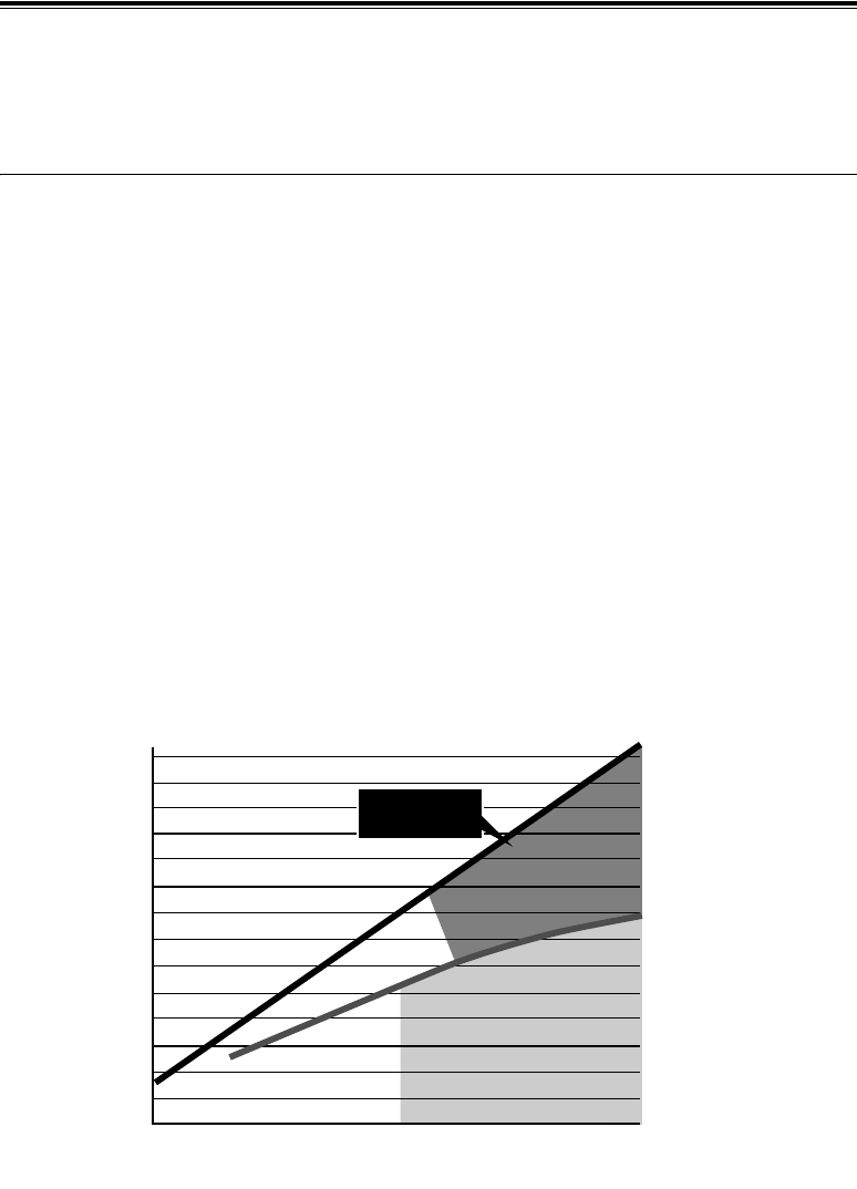
Algorithmic complexity increases as application demands increase. Figure 1-1 illustrates performance
demands over time. In order to process these new algorithms, higher-performance signal processing
engines are required. Typical fixed architecture DSP processors cannot keep pace on their own. A DSP
co-processor is often needed to handle the highest performance portions of these ever increasingly
complex algorithms. The “performance gap” in Figure 1-1 illustrates this expanding co-processing
requirement.
Figure 1-1: The Performance Gap
DSP/GPP*
Traditional
Processor
Architectures
Performance
(Algorithm and Processor Forecast)
Algorithm Complexity
4G
3G
Imaging
Radar
SD/HD Video
SDR
*Source: Jan Rabaey, BWRC
1960 1970 1980 1990 2000 2010
Performance
Gap

DSP: DESIGNING FOR OPTIMAL RESULTS
2 • Xilinx
Field Programmable Gate Arrays (FPGAs) are very well suited to fill the performance gap for a
variety of reasons:
• They offer extremely high-performance signal processing capability through parallelism.
• They provide very low risk due to the flexible architecture.
• They allow design migration to handle changing standards.
• Developers can use them to create a customized and differentiated solution.
• They are quickly coming down in price. In fact, it is possible to find FPGAs for less then $2
per device.
• They provide very low power per function.
The Ideal Solution
With the revolutionary XtremeDSP™ Slices, Xilinx Virtex™-4 FPGAs deliver the ideal solution for
high-performance digital signal processing. They satisfy high-performance signal processing tasks
traditionally serviced by an ASIC or ASSP. They allow you to create high-performance DSP engines
that can boost the signal processing performance of your system for a host of applications including
digital communications and video/imaging. And they are the ideal choice to increase system level
performance by complementing a programmable DSP system as either a pre- or co-processor.
XtremeDSP Slice Delivers Maximum Performance, Minimum Power,
and Best Economy
The XtremeDSP™ Slice⎯operating at a blazing 500 MHz⎯lies at the heart of Virtex-4 FPGA’s
XtremeDSP performance. As the most powerful addition to the Xilinx XtremeDSP
took kit, it is a
unique piece of hard coded IP embedded in each Virtex-4 device. It provides industry-leading DSP
processing performance, unrivalled economy, and the lowest power consumption of any device in this
performance range.
Simplicity and Efficiency of the Cascade Logic
The built-in cascade logic of the XtremeDSP Slice allows multiple slices to be connected together to
implement complex filters and multi-precision functions while operating at full speed. And the
cascade logic provides tremendous cost advantage. Other solutions require additional FPGA resources
to build costly and inefficient adder trees to implement this common function. They require a much
larger FPGA to implement the same level of functionality that can be attained in an XtremeDSP-
enabled Virtex-4 FPGA. The result is a tremendous performance and cost advantage of the Virtex-4
device over other FPGA DSP solutions.
Extremely Low Power Consumption
Each XtremeDSP Slice consumes only 2.3 mW/100 MHz in a typical system implementation. This
extremely low power is enabled by the optimized hard implementation of the XtremeDSP Slice. Also,
the programmable logic fabric of the Virtex-4 family has a significant power advantage. For example,
power-per-CLB has been cut in half, with static power reduced by 40% and dynamic power reduced by
50%. In addition, certain hard-logic silicon functions in the Virtex-4 FPGA reduce consumption by
approximately 90%. This results in a lower power budget and all its associated benefits⎯higher
reliability, smaller power devices, smaller fans, and so on.

DIGITAL SIGNAL PROCESSING DESIGN CHALLENGES
Xilinx • 3
Increased Flexibility for Cost Effectiveness
The Virtex-4 FPGA flexibility boosts cost effectiveness for all application designs. For example,
Virtex-4 FPGAs enable you to buy a customer device that supports two applications⎯one for
diagnostic testing and one for the application. Here, Virtex-4 FPGAs can be tested for two designs or
two variations of the same design. Savings are realized right down the line, from inventory costs, to
design costs, to system costs, to consumer costs.
Easy to Use
Xilinx and its partners provide the easiest-to-use design solutions for FPGA-based DSP solutions with
features such as:
• System Generator for DSP reduces design time.
• A rich DSP IP library implements fast, highly optimized algorithms.
• Award-winning technical support and DSP services enable you to bring products to market
much faster.
Whether you are working with spread-spectrum, multi-carrier, or narrowband communication
systems, Virtex-4 FPGAs are the ideal choice for ease of use.
Virtex-4 FPGAs
⎯
A Platform for Every Application
All Virtex-4 platforms offer XtremeDSP capabilities. Choose the device that provides the optimal
DSP performance for your application:
• Virtex-4 SX devices offer the most cost-effective implementation of ultra-high performance
DSP functionality for high-end DSP applications. They provide the highest ratio of
XtremeDSP slices—up to 512⎯and deliver up to 256 GMACS (18x18-bit multiply, 48-bit
addition/accumulation) performance.
• Virtex-4 LX devices offer ample XtremeDSP slices and include more logic, memory, and I/O
resources for logic applications.
• Virtex-4 FX devices include embedded PowerPC™ processors and RocketIO™ multi-
gigabit transceivers for embedded processing and high-speed serial applications.
XtremeDSP platform solutions accelerate your products’ time-to-market through superior
design, design tools, intellectual property cores, and design services. They provide the fastest means of
designing, verifying, and deploying your DSP algorithms and systems in FPGAs.
Reduce Time-to-Market with World-Class Xilinx Support
Xilinx supplies a host of support functions to designers including DSP training courses, award
winning technical support, technical data, implementation data, and design consulting.
A Must-Read
This book is a must-read for DSP designers who want to tap the power of the Virtex-4 XtremeDSP
Slice. It provides a detailed description of the multiple features of the slice as well as providing
multiple examples that show you how to harness the power and flexibility of this powerful IP block.
Tap into the XtremeDSP Slice and reap the rewards of highest performance, lowest power at the lowest
cost.

DSP: DESIGNING FOR OPTIMAL RESULTS
4 • Xilinx

Xilinx • 5
Chapter 2
XtremeDSP Design Considerations
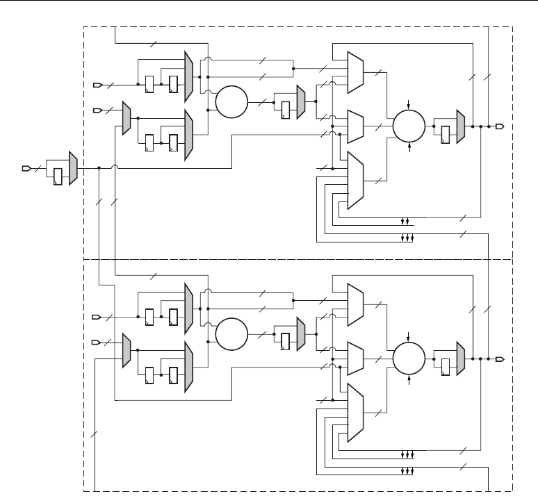
This chapter provides technical details for the XtremeDSP™ Digital Signal Processing (DSP)
element, the DSP48 slice.
The DSP48 slice is a new element in the Xilinx development model referred to as “Application
Specific Modular Blocks” (ASMBL). The purpose of this model is to deliver off-the-shelf
programmable devices with the best mix of logic, memory, I/O, processors, clock management, and
digital signal processing. ASMBL is an efficient FPGA development model for delivering off-the-
shelf, flexible solutions ideally suited to different application domains.
Each XtremeDSP tile contains two DSP48 slices to form the basis of a versatile coarse-grain DSP
architecture. Many DSP designs follow a multiply with addition. In Virtex™-4 devices these elements
are supported in dedicated circuits.
The DSP48 slices support many independent functions, including multiplier, multiplier-
accumulator (MAC), multiplier followed by an adder, three-input adder, barrel shifter, wide bus
multiplexers, magnitude comparator, or wide counter. The architecture also supports connecting
multiple DSP48 slices to form wide math functions, DSP filters, and complex arithmetic without the
use of general FPGA fabric.
The DSP48 slices available in all Virtex-4 family members support new DSP algorithms and
higher levels of DSP integration than previously available in FPGAs. Minimal use of general FPGA
fabric leads to low power, very high performance, and efficient silicon utilization.
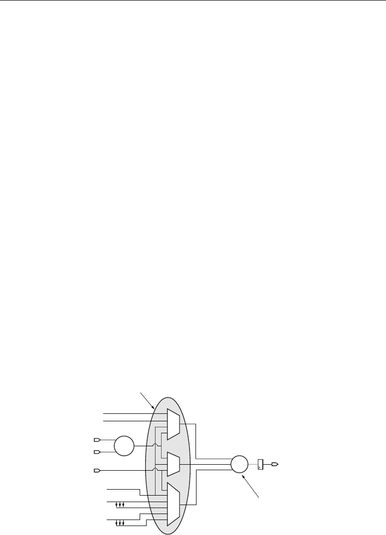
Introduction
The DSP48 slices facilitate higher levels of DSP integration than previously possible in FPGAs. Many
DSP algorithms are supported with minimal use of the general-purpose FPGA fabric, resulting in low
power, high performance, and efficient device utilization.
At first look, the DSP48 slice is an 18 x 18 bit two’s complement multiplier followed by a 48-bit
sign-extended adder/subtracter/accumulator, a function that is widely used in digital signal processing
(DSP).
A second look reveals many subtle features that enhance the usefulness, versatility, and speed of
this arithmetic building block.
Programmable pipelining of input operands, intermediate products, and accumulator outputs
enhances throughput. The 48-bit internal bus allows for practically unlimited aggregation of DSP
slices.

DSP: DESIGNING FOR OPTIMAL RESULTS
6 • Xilinx
One of the most important features is the ability to cascade a result from one XtremeDSP Slice to
the next without the use of general fabric routing. This path provides high-performance and low-
power post addition for many DSP filter functions of any tap length.
For multi-precision arithmetic this path supports a right-wire-shift. Thus a partial product from
one XtremeDSP Slice can be right-justified and added to the next partial product computed in an
adjacent such slice. Using this technique, the XtremeDSP Slices can be configured to support any size
operands.
Another key feature for filter composition is the ability to cascade an input stream from slice to
slice.
The C input port, allows the formation of many 3-input mathematical functions, such as 3-input
addition, 2-input multiplication with a single addition. One subset of this function is the very
valuable support of rounding a multiplication “away from zero”.
Architecture Highlights
The Virtex-4 DSP slices are organized as vertical DSP columns. Within the DSP column, two vertical
DSP slices are combined with extra logic and routing to form a DSP tile. The DSP tile is four CLBs
tall.
Each DSP48 slice has a two-input multiplier followed by multiplexers and a three-input
adder/subtracter. The multiplier accepts two 18-bit, two's complement operands producing a 36-bit,
two's complement result. The result is sign extended to 48 bits and can optionally be fed to the
adder/subtracter. The adder/subtracter accepts three 48-bit, two's complement operands, and produces
a 48-bit two's complement result.
Higher level DSP functions are supported by cascading individual DSP48 slices in a DSP48
column. One input (cascade B input bus) and the DSP48 slice output (cascade P output bus) provide
the cascade capability. For example, a Finite Impulse Response (FIR) filter design can use the
cascading input to arrange a series of input data samples and the cascading output to arrange a series
of partial output results. For details on this technique, refer to the section titled “Adder Cascade vs.
Adder Tree,” page 31.
Architecture highlights of the DSP48 slices are:
• 18-bit by 18-bit, two's-complement multiplier with a full-precision 36-bit result, sign
extended to 48 bits
• Three-input, flexible 48-bit adder/subtracter with optional registered accumulation feedback
• Dynamic user-controlled operating modes to adapt DSP48 slice functions from clock cycle to
clock cycle
• Cascading 18-bit B bus, supporting input sample propagation
• Cascading 48-bit P bus, supporting output propagation of partial results
• Multi-precision multiplier and arithmetic support with 17-bit operand right shift to align
wide multiplier partial products (parallel or sequential multiplication)
• Symmetric intelligent rounding support for greater computational accuracy
• Performance enhancing pipeline options for control and data signals are selectable by
configuration bits
• Input port “C” typically used for multiply-add operation, large three-operand addition, or
flexible rounding mode
• Separate reset and clock enable for control and data registers
XTREMEDSP DESIGN CONSIDERATIONS
Xilinx • 7
• I/O registers, ensuring maximum clock performance and highest possible sample rates with
no area cost
• OPMODE multiplexers
A number of software tools support the DSP48 slice. The Xilinx ISE software supports DSP48
slice instantiations. The Architecture Wizard is a GUI for creating instantiation VHDL and/or Verilog
code. It also helps generate code for designs using a single DSP48 slice (i.e., Multiplier, Adder,
Multiply-Accumulate or MAC, and Dynamic Control modes). Using the Architecture Wizard, CORE
Generator™ tool, or System Generator, a designer can quickly generate math or other functions using
Virtex-4 DSP48 slices.
Number of DSP48 Slices Per Virtex-4 Device
Table 2-1 shows the number of DSP48 slices for each device in the Virtex-4 families. The Virtex-4 SX
family offers the highest ratio of DSP48 slices to logic, making it ideal for math-intensive
applications.
Table 2-1: Number of DSP48 Slices per Family Member
Device DSP48 Device DSP48 Device DSP48
XC4VLX15 32 XC4VFX12 32
XC4VLX25 48 XC4VSX25 128 XC4VFX20 32
XC4VSX35 192
XC4VLX40 64 XC4VFX40 48
XC4VLX60 64 XC4VSX55 512 XC4VFX60 128
XC4VLX80 80
XC4VLX100 96 XC4VFX100 160
XC4VLX160 96
XC4VLX200 96 XC4VFX140 192
DSP: DESIGNING FOR OPTIMAL RESULTS
8 • Xilinx
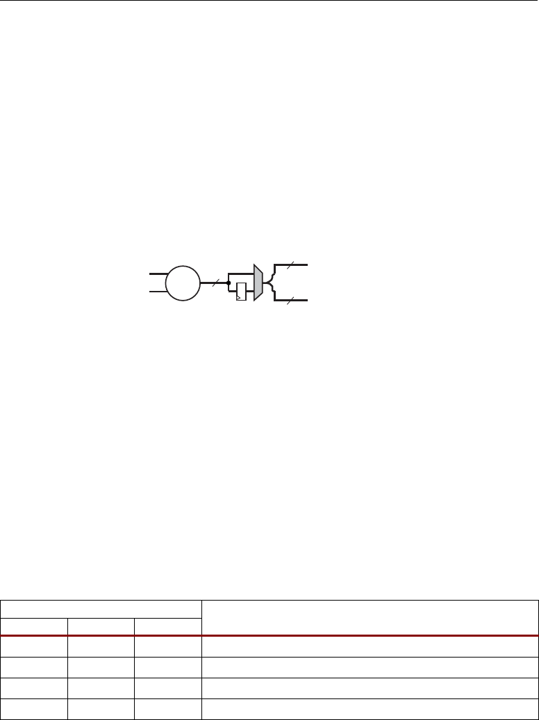
DSP48 Slice Primitive
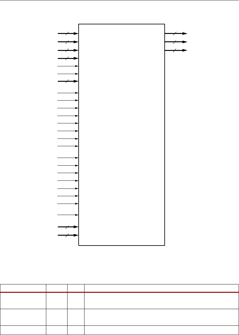
Figure 2-1 shows the DSP48 slice primitive.
Table 2-2 lists the available ports in the DSP48 slice primitive.
Figure 2-1: DSP48 Slice Primitive
Table 2-2: DSP48 Slice Port List and Definitions
Signal Name Direction Size Function
A
I18
The multiplier's A input. This signal can also be used as the
adder's Most Significant Word (MSW) input
B
I18
The multiplier's B input. This signal can also be used as the
adder's Least Significant Word (LSW) input
C
I48
The adder's C input
A[17:0]
B[17:0]
C[47:0]
OPMODE[6:0]
SUBTRACT
CARRYIN
CARRYINSEL[1:0]
BCIN[17:0]
PCIN[47:0]
CLK
CEA
BCOUT[17:0]
P[47:0]
PCOUT[47:0]
18
18
48
7
2
18
48
18
48
48
CEB
CEC
CEP
CECTRL
CECINSUB
RSTA
RSTB
RSTC
RSTP
RSTCTRL
RSTCARRYIN
CEM
RSTM
CECARRYIN
ug073_c1_01_060304

XTREMEDSP DESIGN CONSIDERATIONS
Xilinx • 9
OPMODE
I7
Controls the input to the X, Y, and Z multiplexers in the DSP48
slices (see OPMODE, Table 2-7)
SUBTRACT
I1
0=add, 1=subtract
CARRYIN
I1
The carry input to the carry select logic
CARRYINSEL
I2
Selects carry source (see CARRYINSEL, Table 2-8)
CEA
I1
Clock enable: 0 = hold, 1 = enable AREG
CEB
I1
Clock enable: 0 = hold, 1 = enable BREG
CEC
I1
Clock enable: 0 = hold, 1 = enable CREG
CEM
I1
Clock enable: 0 = hold, 1 = enable MREG
CEP
I1
Clock enable: 0 = hold, 1 = enable PREG
CECTRL
I1
Clock enable: 0 = hold, 1 = enable OPMODEREG,
CARRYINSELREG
CECINSUB
I1
Clock enable: 0 = hold, 1 = enable SUBTRACTREG and
general interconnect carry input
CECARRYIN
I1
Clock enable: 0 = hold, 1 = enable (carry input from internal
paths)
RSTA
I1
Reset: 0 = no reset, 1 = reset AREG
RSTB
I1
Reset: 0 = no reset, 1 = reset BREG
RSTC
I1
Reset: 0 = no reset, 1 = reset CREG
RSTM
I1
Reset: 0 = no reset, 1 = reset MREG
RSTP
I1
Reset: 0 = no reset, 1 = reset PREG
RSTCTRL
I1
Reset: 0 = no reset, 1 = reset SUBTRACTREG,
OPMODEREG, CARRYINSELREG
RSTCARRYIN
I1
Reset: 0 = no reset, 1 = reset (carry input from general
interconnect and internal paths)
CLK
I1
The DSP48 clock
BCIN
I18
The multiplier's cascaded B input. This signal can also be used
as the adder's LSW input
PCIN
I48
Cascaded adder's Z input from the previous DSP slice
BCOUT
O18
The B cascade output
PCOUT
O48
The P cascade output
P
O48
The product output
Table 2-2: DSP48 Slice Port List and Definitions (Continued)
Signal Name Direction Size Function

DSP: DESIGNING FOR OPTIMAL RESULTS
10•Xilinx
DSP48 Slice Attributes
The synthesis attributes for the DSP48 slice are described in detail throughout this section. With the
exception of the B_INPUT and LEGACY_MODE attributes, all other attributes call out pipeline
registers in the control and datapaths. The value of the attribute sets the number of pipeline registers.
The attribute settings are as follows:
• The AREG and BREG attributes can take a value of 0, 1, or 2. The values define the number
of pipeline registers in the A and B input paths. See the “A, B, C, and P Port Logic” section
for more information.
• The CREG, MREG, and PREG attributes can take a value of 0 or 1. The value defines the
number of pipeline registers at the output of the multiplier (MREG) (shown in Figure 2-11)
and at the output of the adder (PREG) (shown in Figure 2-9). The CREG attribute is used to
select the pipeline register at the 'C' input (shown in Figure 2-8).
• The CARRYINREG, CARRYINSELREG, OPMODEREG, and SUBTRACTREG attributes
take a value of 0 if there is no pipelining register on these paths, and take a value of 1 if there
is one pipeline register in their path. The CARRYINSELREG, OPMODEREG, and
SUBTRACTREG paths are shown in Figure 2-10, and the CARRYINREG path is shown in
Figure 2-12.
• The B_INPUT attribute defines whether the input to the B port is routed from the parallel
input (attribute: DIRECT) or the cascaded input from the previous slice (attribute:
CASCADE).
• The LEGACY_MODE attribute serves two purposes. The first purpose is similar in nature to
the MREG attribute. It defines whether or not the multiplier is "flow through" in nature (i.e.,
LEGACY_MODE value equal to MULT18x18) or contains a single pipeline register in the
middle of the multiplier (i.e., LEGACY_MODE value equal to MULT18x18S is the same as
MREG value equal to one). While this is redundant to the MREG attribute, it was deemed
useful for customers used to the Virtex-II and Virtex-II Pro multipliers since the DSP48 setup
and hold timing most closely matches those of the Virtex-II and Virtex-II Pro MULT18x18S
when the MREG is used. Any disagreement between the MREG attribute and
LEGACY_MODE attribute settings are flagged as a software Design Rule Check (DRC) error.
The second purpose for the attribute is to convey to the timing tools whether the A and B port
through the combinatorial multiplier path (slower timing) or faster X multiplexer bypass
path for A:B should be used in the timing calculations. Since the OPMODE can change
dynamically, the timing tools cannot determine this without an attribute.
To summarize the timing tools behavior:
♦ If (attribute: NONE), then timing analysis/simulation bypasses the multiplier for the
highest performance. The lowest power dissipation is achieved by setting MREG to one
while CEM input is grounded.
♦ If (attribute: MULT18x18), then timing analysis/simulation uses the combinatorial path
through the multiplier. In this case, MREG must be set to zero or a DRC error occurs.
♦ If (attribute: MULT18x18S), then timing analysis/simulation uses a pipelined multiplier.
In this case MREG must be set to one or a DRC error occurs.

XTREMEDSP DESIGN CONSIDERATIONS
Xilinx • 11
Attributes in VHDL
DSP48 generic map (
AREG => 1,-- Number of pipeline registers on the A input, 0, 1 or 2
BREG => 1,-- Number of pipeline registers on the B input, 0, 1 or 2
B_INPUT => “DIRECT”, -- B input DIRECT from fabric or CASCADE from
-- another DSP48
CARRYINREG => 1, -- Number of pipeline registers for the CARRYIN
-- input, 0 or 1
CARRYINSELREG => 1, -- Number of pipeline registers for the
-- CARRYINSEL, 0 or 1
CREG => 1, -- Number of pipeline registers on the C input, 0 or 1
LEGACY_MODE => “MULT18X18S”, -- Backward compatibility, NONE,
-- MULT18X18 or MULT18X18S
MREG => 1, -- Number of multiplier pipeline registers, 0 or 1
OPMODEREG => 1,-- Number of pipeline registers on OPMODE input,
-- 0 or 1
PREG => 1, -- Number of pipeline registers on the P output, 0 or 1
SIM_X_INPUT => “GENERATE_X_ONLY”,
-- Simulation parameter for behavior for X on input.
-- Possible values: GENERATE_X, NONE or WARNING
SUBTRACTREG => 1)-- Number of pipeline registers on the SUBTRACT
-- input, 0 or 1
Attributes in Verilog
defparam DSP48_inst.AREG = 1;
// Number of pipeline registers on the A input, 0, 1 or 2
defparam DSP48_inst.BREG = 1;
// Number of pipeline registers on the B input, 0, 1 or 2
defparam DSP48_inst.B_INPUT = “DIRECT”;
// B input DIRECT from fabric or CASCADE from another DSP48
defparam DSP48_inst.CARRYINREG = 1;
// Number of pipeline registers for the CARRYIN input, 0 or 1
defparam DSP48_inst.CARRYINSELREG = 1;
// Number of pipeline registers for the CARRYINSEL, 0 or 1
defparam DSP48_inst.CREG = 1;
// Number of pipeline registers on the C input, 0 or 1
defparam DSP48_inst.LEGACY_MODE = “MULT18X18S”;
// Backward compatibility, NONE, MULT18X18 or MULT18X18S
defparam DSP48_inst.MREG = 1;
// Number of multiplier pipeline registers, 0 or 1
defparam DSP48_inst.OPMODEREG = 1;
// Number of pipeline registers on OPMODE input, 0 or 1
defparam DSP48_inst.PREG = 1;
// Number of pipeline registers on the P output, 0 or 1
defparam DSP48_inst.SIM_X_INPUT = “GENERATE_X_ONLY”;
// Simulation parameter for behavior for X on input.
// Possible values: GENERATE_X, NONE or WARNING
defparam DSP48_inst.SUBTRACTREG = 1;
// Number of pipeline registers on the SUBTRACT input, 0 or 1
DSP: DESIGNING FOR OPTIMAL RESULTS
12•Xilinx
DSP48 Tile and Interconnect
Two DSP48 slices, a shared 48-bit C bus, and dedicated interconnect form a DSP48 tile. The DSP48
tiles stack vertically in a DSP48 column. The height of a DSP48 tile is the same as four CLBs and also
matches the height of one block RAM. This “regularity” enhances the routing of wide datapaths.
Smaller Virtex-4 family members have one DSP48 column while the larger Virtex-4 family members
have two, four, or eight DSP48 columns.
As shown in Figure 2-2, the multipliers and block RAM share interconnect resources in the
Virtex-II and Virtex-II Pro architectures. Virtex-4 devices, however, have independent routing for the
DSP48 tiles and block RAM, effectively doubling the available data bandwidth between the elements.
Figure 2-3 shows two DSP48 slices and their associated datapaths stacked vertically in a DSP48
column. The inputs to the shaded multiplexers are selected by configuration control signals. These are
set by attributes in the HDL source code or by the User Constraint File (UCF).
Figure 2-2: DSP48 Interconnect and Relative Dedicated Element Sizes
Multiplier BRAM
BRAM
DSP48
Slice
DSP48
Slice
Virtex-4 Devices
Virtex-II and Virtex-II Pro Devices
ug073_c1_02_060304
Interconnect
Interconnect Interconnect
XTREMEDSP DESIGN CONSIDERATIONS
Xilinx • 13
Notes:
1. The 18-bit A bus and B bus are concatenated, with the A bus being the most significant.
2. The X,Y, and Z multiplexers are 48-bit designs. Selecting any of the 36-bit inputs provides a
48-bit sign-extended output.
3. The multiplier outputs two 36-bit partial products, sign extended to 48 bits. The partial
products feed the X and Y multiplexers. When OPMODE selects the multiplier, both X and Y
multiplexers are utilized and the adder/subtracter combines the partial products into a valid
multiplier result.
4. The multiply-accumulate path for P is through the Z multiplexer. The P feedback through the X
multiplexer enables accumulation of P cascade when the multiplier is not used.
5. The “Right Wire Shift by 17 bits” path truncates the lower 17 bits and sign extends the upper 17
bits.
6. The grey-colored multiplexers are programmed at configuration time.
7. The shared C register supports multiply-add, wide addition, or rounding.
8. Enabling SUBTRACT implements Z – (X+Y+CIN) at the output of the adder/subtracter.
Figure 2-3: A DSP48 Tile Consisting of Two DSP48 Slices
Zero
Note 2
A
B
PCINBCIN
P
18
18
18
18
48 48
48
48
36
48
48
48
X
BCOUT PCOUT
Z
72
Note 1
18
18
36
36
48
48
Note 3
Note 4
Notes 4, 5
Wire Shift Right by 17 bits
±
×
Zero
Note 2
C
A
B
PCINBCIN
P
18
18
48
1848
18
48 48
48
48
36
48
48
48
Y
X
BCOUT PCOUT
Z
72
Note 1
18
18
36
36
48
48
Note 3
Note 4
Notes 4, 5
Note 5
Note 5
Wire Shift Right by 17 bits
ug073_c1_03_020405
±
×
Y
SUBTRACT
Note 8
CIN
SUBTRACT
Note 8
CIN
Note 7
DSP: DESIGNING FOR OPTIMAL RESULTS
14•Xilinx
Simplified DSP48 Slice Operation
The math portion of the DSP48 slice consists of an 18-bit by 18-bit, two’s complement multiplier
followed by three 48-bit datapath multiplexers (with outputs X, Y, and Z) followed by a three-input,
48-bit adder/subtracter.
The data and control inputs to the DSP48 slice feed the arithmetic portions directly, or are
optionally registered one or two times to assist the construction of different, highly pipelined, DSP
application solutions. The data inputs A and B can be registered once or twice. The other data inputs
and the control inputs can be registered once. Full speed operation is 500 MHz when using the
pipeline registers. More detailed timing information is available in the Timing Section.
In its most basic form the output of the adder/subtracter is a function of its inputs. The inputs are
driven by the upstream multiplexers, carry select logic, and multiplier array. Equation 2-1
summarizes the combination of X, Y, Z, and CIN by the adder/subtracter. The CIN, X multiplexer
output, and Y multiplexer output are always added together. This combined result can be selectively
added to or subtracted from the Z multiplexer output.
Adder Out = (Z ± (X + Y + CIN)) Equation 2-1
Equation 2-2 describes a typical use where A and B are multiplied and the result is added to or
subtracted from the C register. More detailed operations based on control and data inputs are described
in later sections. Selecting the multiplier function consumes both X and Y multiplexer outputs to feed
the adder. The two 36-bit partial products from the multiplier are sign extended to 48 bits before
being sent to the adder/subtracter.
Adder Out = C ± (A × B+CIN) Equation 2-2
Figure 2-4 shows the DSP48 slice in a very simplified form. The seven OPMODE bits control the
selection of the 48-bit datapaths by the three multiplexers feeding each of the three inputs to the
adder/subtracter. In all cases, the 36-bit input data to the multiplexers is sign extended, forming 48-
bit input datapaths to the adder/subtracter. Based on 36-bit operands and a 48-bit accumulator
output, the number of “guard bits” (i.e., bits available to guard against overflow) is 12. Therefore, the
number of multiply accumulations possible before overflow occurs is 4096. Combinations of
OPMODE, SUBTRACT, CARRYINSEL, and CIN control the function of the adder/subtracter.
Figure 2-4: Simplified DSP48 Slice Model
±
×
A:B
P
Zero
B
PCIN
P
Y
X
Z
A
C
P
OPMODE
Controls
Behavior
OPMODE, CARRYINSEL, CIN,
and SUBTRACT Control Behavior
UG073_c1_04_070904

XTREMEDSP DESIGN CONSIDERATIONS
Xilinx • 15
Timing Model
Table 2-3 lists the XtremeDSP switching characteristics.
Table 2-3: XtremeDSP Switching Characteristics
Symbol Description Function
Control
Signal
Setup and Hold of CE Pins
T
DSPCCK_CE
/T
DSPCKC_CE
Setup/Hold of all CE inputs of the
DSP48 slice
Clock
Enable
CE
T
DSPCCK_RST
/T
DSPCKC_RST
Setup/Hold of all RST inputs of the
DSP48 slice
Reset RST
Setup and Hold Times of Data/Control Pins
T
DSPDCK_{AA, BB, CC}
/
T
DSPCKD_{AA, BB, CC}
Setup/Hold of {A, B, C} input to {A, B,
C} register
Data In A, B, C
T
DSPDCK_{AM, BM}
/
T
DSPCKD_{AM, BM}
Setup/Hold of {A, B} input to M register
Data In A, B
T
DSPDCK_{AP, BP}_L
/
T
DSPCKD_{AP, BP}_L
Setup/Hold of {A, B} input to P register
(LEGACY_MODE = MULT18X18)
Data In A, B
T
DSPDCK_{AP_NL, BP_NL, CP}
/
T
DSPCKD_{AP_NL, BP_NL, CP}
Setup/Hold of {A, B, C} input to P
register (LEGACY_MODE = NONE
for A and B)
Data In A, B, C
T
DSPDCK_{CRYINC, CRYINSC,
OPO, SUBS}
/
T
DSPCKD_{CRYINC, CRYINSC,
OPO, SUBS}
Setup/Hold of {CARRYIN,
CARRYINSEL, OPMODE,
SUBTRACT} input to {CARRYIN,
CARRYINSEL, OPMODE,
SUBTRACT} register
Control In Various
T
DSPDCK_{CRYINP, CRYINSP,
OPP, SUBPPCINP}
/
T
DSPCKD_{CRYINP, CRYINSP,
OPP, SUBP, PCINP}
Setup/Hold of {CARRYIN,
CARRYINSEL, OPMODE,
SUBTRACT, PCIN} input to P register
Control In Various
Clock to Out
T
DSPCKO_PP
Clock to out from P register to P output
Data Out P Output
T
DSPCKO_{PA, PB}_L
Clock to out from {A, B} register to P
output
(LEGACY_MODE = MULT18X18)
Data Out P Output
T
DSPCKO_{PA_NL, PB_NL, PC}
Clock to out from {A, B, C} register to P
output (LEGACY_MODE = NONE for
A and B)
Data Out P Output
T
DSPCKO_{PM, PCRYIN,
PCRYINS, POP, PSUB}
Clock to out from {M, CARRYIN,
CARRYINSEL, OPMODE,
SUBTRACT} register to P output
Data Out P Output

DSP: DESIGNING FOR OPTIMAL RESULTS
16•Xilinx
T
DSPCKO_PCOUTP
Clock to out from P register to PCOUT
output
Data Out P Output
T
DSPCKO_{PCOUTA, PCOUTB}_L
Clock to out from {A, B} register to
PCOUT output
(LEGACY_MODE = MULT18X18)
Data Out P Output
T
DSPCKO_{PCOUTA_NL,
PCOUTB_NL, PCOUTC}
Clock to out from {A, B, C} register to
PCOUT output
(LEGACY_MODE = NONE for A and
B)
Data Out P Output
T
DSPCKO_{PCOUTM,
PCOUTCRYIN, PCOUTCRYINS,
PCOUTOP, PCOUTSUB}
Clock to out from {M, CARRYIN,
CARRYINSEL, OPMODE,
SUBTRACT} register to PCOUT output
Data Out P Output
Combinatorial
T
DSPDO_{AP, BP}_L
{A, B} input to P output
(LEGACY_MODE = MULT18X18)
Data In
to Out
A, B to P
T
DSPDO_{AP_NL, BP_NL, CP}
{A, B, C} input to P output
(LEGACY_MODE = NONE for A and
B)
Data In
to Out
A, B, C to
P
T
DSPDO_{CRYINP, CRYINSP,
OPMODEP, SUBTRACTP, PCINP}
{CARRYIN, CARRYINSEL,
OPMODE, SUBTRACT, PCIN} input
to P output
Control to
Data Out
Various
T
DSPDO_{APCOUT, BPCOUT}_L
{A, B} input to PCOUT output
(LEGACY_MODE = MULT18X18)
Data In
to PC Out
A, B to
PC Out
T
DSPDO_{APCOUT_NL,
BPCOUT_NL, CPCOUT}
{A, B, C} input to PCOUT output
(LEGACY_MODE = NONE for A and
B)
Data In
to PC Out
A, B, C to
PC Out
T
DSPDO_{CRYINPCOUT,
CRYINSPCOUT, OPMODEPCOUT,
SUBTRACTPCOUT, PCINPCOUT}
{CARRYIN, CARRYINSEL,
OPMODE, SUBTRACT, PCIN} input
to PCOUT output
Control to
PC Out
Various
Sequential
T
DSPCKCK_{AP, BP}_L
From {A, B} register to P register
(LEGACY_MODE = MULT18X18)
Register to
register
–
T
DSPCKCK_{AP_NL, BP_NL, CP,
PP}
From {A, B, C, P} register to P register
(LEGACY_MODE = NONE for A and
B)
Register to
register
–
Table 2-3: XtremeDSP Switching Characteristics (Continued)
Symbol Description Function
Control
Signal

XTREMEDSP DESIGN CONSIDERATIONS
Xilinx • 17
The timing diagram in Figure 2-5 uses OPMODE equal to
0x05 with all pipeline registers
turned on. For other applications, the clock latencies and the parameter names must be adjusted.
The following events occur in Figure 2-5:
1. At time T
DSPCCK_CE
before CLK event 1, CE becomes valid High to allow all DSP registers to
sample incoming data.
2. At time T
DSPDCK_{AA,BB,CC}
before CLK event 1, data inputs A, B, C have remained stable for
sampling into the DSP slice.
3. At time T
DSPCKO_PP
after CLK event 4, the P output switches into the results of the data
captured at CLK event 1. This occurs three clock cycles after CLK event 1.
T
DSPCKCK_{CRYINP, CRYINSP,
OPMODEP, SUBTRACTP}
From {CARRYIN, CARRYINSEL,
OPMODE, SUBTRACT} register to P
register
Register to
register
–
T
DSPCKCK__{AM, BM}
From {A, B} register to M register
Register to
register
–
Figure 2-5: XtremeDSP Timing Diagram
Table 2-3: XtremeDSP Switching Characteristics (Continued)
Symbol Description Function
Control
Signal
CLK
CE
RST
A Don't Care
CLK Event 1 CLK Event 4 CLK Event 5
Data A1 Data A2 Data A3 Data A4
Don't Care Data B1 Data B2 Data B3 Data B4
Don't Care Data C1 Data C2 Data C3 Data C4
0
B
C
P
T
DSPDCK_CC
T
DSPCKO_CC
T
DSPCKO_CC
UG073_c1_27_071204
T
DSPCCK_RST
T
DSPCCK_CE
T
DSPDCK_AA
T
DSPDCK_BB
Result 1Don't Care

DSP: DESIGNING FOR OPTIMAL RESULTS
18•Xilinx
4. At time T
DSPCCK_RST
before CLK event 5, the RST signal becomes valid High to allow a
synchronous reset at CLK event 5.
5. At time T
DSPCKO_PP
after CLK event 5, the output P becomes a logic 0.
A, B, C, and P Port Logic
The DSP48 slice input and output data ports support many common DSP and math algorithms. The
DSP48 slice has two direct 18-bit input data ports labeled A and B. Two DSP48 slices within a DSP48
tile share a direct 48-bit input data port labeled C. Each DSP48 slice has one direct 48-bit output port
labeled P, a cascaded input datapath (B cascade), and a cascaded output datapath (P cascade), providing
a cascaded input and output stream between adjacent DSP48 slices. Applications benefiting from this
feature include FIR filters, complex multiplication, multi-precision multiplication, complex MACs,
adder cascade, and adder tree (the final summation of several multiplier outputs) support.
The 18-bit A and B port can supply input data to the 18-bit by 18-bit, two's complement
multiplier. A and B concatenated can bypass the multiplier and feed the X multiplexer input. The 48-
bit C port is used as a general input to the Y and Z multiplexer to perform multiply, add, subtract,
three-input add/subtract functions, or rounding.
Multiplexers controlled by configuration bits select flow through paths, optional registers, or
cascaded inputs. The data port registers allow users to typically trade off increased clock frequency
(i.e., higher performance) vs. data latency. There is also a configuration controlled pipeline register
between the multiplier and adder/subtracter known as the M register. The registers have independent
clock enables and resets as described in Table 2-2 and shown in Figure 2-1.
The configuration bit enables the C register to select between two potentially different clock
domains as shown in Figure 2-8, page 19. The selection of the clock multiplexer is not set by user
attributes. If the C register is used, the DSP48 slices packed in the same DSP48 tile must either be in
the same clock domain or meet multicycle clock constraints.
The shared “C” input within the DSP tile can be used by the two slices within a tile in any one of
the following modes:
1. Neither DSP48 slice uses the C port.
The C inputs in both the slices are connected to GND, “0” in the HDL code. The place and route
software maps the two slices in one tile.
2. Both DSP48 slices use the same C port inputs.
The C inputs in both the slices are connected to “C” in the HDL code. The place and route
software maps the two slices in one tile.
3. Only one DSP48 slice uses the C port.
In this case, the C input on slice 1 is connected to “C”, and the C input on slice 2 is connected to
“0” in the HDL code. A C port connected to “0” is taken as an unused C port in the software. The
software can map the two slices in one tile. The simulation shows the C input connected to “0” for
slice 2 in the code. However, in the hardware, the C port on slice 2 is connected to the C port on
slice 1, causing a potential simulation mismatch for the C port on slice 2. To avoid this potential
mismatch, the C port must not be selected on the Y and Z multiplexers of slice 2. To get a “0” at
the output of multiplexers Y and Z, choose the “0” input of these multiplexers using OPMODE.
Do not use the “C” input to get a zero at the output of Y and Z multiplexers on slice 2.
XTREMEDSP DESIGN CONSIDERATIONS
Xilinx • 19
The A, B, C, and P port logics are shown in Figure 2-6, Figure 2-7, Figure 2-8, and Figure 2-9,
respectively.
Figure 2-6: A Input Logic
Figure 2-7: B Input Logic
Figure 2-8: C Input Logic
RST
EN
DQ
A
18
18
18
18
18
RST
EN
DQ
RSTA
CEA
A input to
Multiplier
UG073_c1_05_061304
B input to
Multiplier
RST
EN
DQ
18
B
18
18
18
18
18
RST
EN
DQ
RSTB
CEB
BCIN
UG073_c1_06_061304
RST
EN
DQ
CLK_0
48
48
48
RSTC
CEC
CLK_1
C
To Both DSP48 Slices
UG073_c1_07_061304

DSP: DESIGNING FOR OPTIMAL RESULTS
20•Xilinx
OPMODE, SUBTRACT, and CARRYINSEL Port Logic
The OPMODE, SUBTRACT, and CARRYINSEL port logic supports flowthrough or registered input
control signals. Similar to the datapaths, multiplexers controlled by configuration bits select
flowthrough or optional registers. The control port registers allow users to trade off increased clock
frequency (i.e., higher performance) vs. data latency.
The registers have independent clock enables and resets as described in Table 2-2 and shown in
Figure 2-1. The OPMODE, SUBTRACT, and CARRYINSEL registers are reset by RSTCTRL. The
SUBTRACT register has a separate enable labeled CECINSUB from OPMODE and CARRYINSEL.
This enable signal is also used to enable the carry input from the general interconnect described in the
“Carry Input Logic” subsection.
Figure 2-10 shows the OPMODE, SUBTRACT, and CARRYINSEL port logic.
Figure 2-9: P Output Logic
Figure 2-10: OPMODE, SUBTRACT, and CARRYINSEL Port Logic
RST
EN
DQ
48
48
48
RSTP
CEP
P
DSP48 Slice Output
UG073_c1_08_061304
To the X, Y, Z Multiplexers and
Carry Input Select Logic
To Adder/Subtracter
CARRYINSEL
RST
EN
DQ
7
SUBTRACT
OPMODE
RST
EN
DQ
2
CECTRL
RSTCTRL
7
2
RST
EN
DQ
CECINSUB
To Carry Input Select Logic
ug073_c1_09_070904
XTREMEDSP DESIGN CONSIDERATIONS
Xilinx • 21
Two’s Complement Multiplier
The two's complement multiplier inside the DSP48 slice accepts two 18-bit x 18-bit two's
complement inputs and produces a 36-bit two's complement result. Cascading of multipliers to
achieve larger products is supported with a 17-bit right-shifted cascaded bus input to the
adder/subtracter to “right justify” partial products by the correct number of bits. MAC functions can
also “right justify” intermediate results for multi-precision. The multiplier can emulate unsigned
math by setting the MSB of an 18-bit operand to zero.
The output of the multiplier consists of two 36-bit partial products. The 36-bit partial products
are sign extended to 48 bits prior to being input to the adder/subtracter. Selecting the output of the
multiplier consumes both X and Y multiplexers whereby the adder/subtracter combines the partial
products to form the final result.
Figure 2-11 shows an optional pipeline register (MREG) for the output of the multiplier. Using
the register provides increased performance with a single clock cycle of increased latency. The grey
multiplexer indicates “selected at configuration time by configuration bits”.
X, Y, and Z Multiplexer
The Operating Mode (OPMODE) inputs provide a way for the design to change its functionality from
clock cycle to clock cycle (e.g., when altering the initial or final state of the DSP48 relative to the
middle part of a given calculation). The OPMODE bits can be optionally registered under the control
of the configuration memory cells (as denoted by the grey colored MUX symbol in Figure 2-10).
Table 2-4, Table 2-5, and Table 2-6 list the possible values of OPMODE and the resulting
function at the outputs of the three multiplexers (X, Y, and Z multiplexers). The multiplexer outputs
supply three operands to the following adder/subtracter. Not all possible combinations for the
multiplexer select bits are allowed. Some are marked in the tables as “illegal selection” and give
undefined results. If the multiplier output is selected, then both the X and Y multiplexers are
consumed supplying the multiplier output to the adder/subtracter.
Figure 2-11: Two’s Complement Multiplier Followed by Optional MREG
Table 2-4: OPMODE Control Bits Select X, Y, and Z Multiplexer Outputs
OPMODE Binary
X Multiplexer Output Fed to Add/Subtract
ZYX
XXX XX 00
ZERO (Default)
XXX 01 01
Multiplier Output (Partial Product 1)
XXX XX 10
P
XXX XX 11
A concatenate B
72
36
36
A
B
Partial Product 1
Partial Product 2
Optional
MREG
ug073_c1_10_070904
×
DSP: DESIGNING FOR OPTIMAL RESULTS
22•Xilinx
There are seven possible non-zero operands for the three-input adder as selected by the three
multiplexers, and the 36-bit operands are sign extended to 48 bits at the multiplexer outputs:
1. Multiplier output, supplied as two 36-bit partial products
2. Multiplier bypass bus consisting of A concatenated with B
3. C bus, 48 bits, shared by two slices
4. Cascaded P bus, 48 bits, from a neighbor DSP48 slice
5. Registered P bus output, 48 bits, for accumulator functions
6. Cascaded P bus, 48 bits, right shifted by 17 bits from a neighbor DSP48 slice
7. Registered P bus output, 48 bits, right shifted by 17 bits, for accumulator functions
Three-Input Adder/Subtracter
The adder/subtracter output is a function of control and data inputs. OPMODE, as shown in the
previous section, selects the inputs to the X, Y, Z multiplexer directed to the associated three
adder/subtracter inputs. It also describes how selecting the multiplier output consumes both X and Y
multiplexers.
As with the input multiplexers, the OPMODE bits specify a portion of this function. Table 2-7
shows OPMODE combinations and the resulting functions. The symbol ± in the table means either
add or subtract and is specified by the state of the SUBTRACT control signal (SUBTRACT = 1 is
defined as “subtraction”). The symbol : in the table means concatenation. The outputs of the X and Y
Table 2-5: OPMODE Control Bits Select X, Y, and Z Multiplexer Outputs
OPMODE Binary
Y Multiplexer Output Fed to Add/Subtract
ZYX
XXX 00 XX
ZERO (Default)
XXX 01 01
Multiplier Output (Partial Product 2)
XXX 10 XX
Illegal selection
XXX 11 XX
C
Table 2-6: OPMODE Control Bits Select X, Y, and Z Multiplexer Outputs
OPMODE Binary
Z Multiplexer Output Fed to Add/Subtract
ZYX
000 XX XX
ZERO (Default)
001 XX XX
PCIN
010 XX XX
P
011 XX XX
C
100 XX XX
Illegal selection
101 XX XX
Shift (PCIN)
110 XX XX
Shift (P)
111 XX XX
Illegal selection

XTREMEDSP DESIGN CONSIDERATIONS
Xilinx • 23
multiplexer and CIN are always added together. This result is then added to or subtracted from the
output of the Z multiplexer.
Table 2-7: OPMODE Control Bits Adder/Subtracter Function
Hex
OPMODE
Binary OPMODE XYZ Multiplexer Outputs and Adder/Subtracter Output
[6:0] Z Y X Z Y X Adder/Subtracter Output
0x00 000 00 00 0
00
±CIN
0x02 000 00 10 0
0
P
±(P + CIN)
0x03 000 00 11 0
0
A:B
±(A:B + CIN)
0x05 000 01 01 0 Note 1
±(A × B+CIN)
0x0c 000 11 00 0 C
0
±(C + CIN)
0x0e 000 11 10 0 C P
±(C + P + CIN)
0x0f 000 11 11 0 C A:B
±(A:B+C+CIN)
0x10 001 00 00 PCIN
00
PCIN ± CIN
0x12 001 00 10 PCIN
0
P
PCIN ± (P + CIN)
0x13 001 00 11 PCIN
0
A:B
PCIN ± (A:B + CIN)
0x15 001 01 01 PCIN Note 1
PCIN ± (A × B+CIN)
0x1c 001 11 00 PCIN C
0
PCIN ± (C + CIN)
0x1e 001 11 10 PCIN C P
PCIN ± (C + P + CIN)
0x1f 001 11 11 PCIN C A:B
PCIN±(A:B+C+CIN)
0x20 010 00 00 P
00
P±CIN
0x22 010 00 10 P
0
P
P±(P+CIN)
0x23 010 00 11 P
0
A:B
P±(A:B+CIN)
0x25 010 01 01 P Note 1
P±(A× B+CIN)
0x2c 010 11 00 P C
0
P±(C+CIN)
0x2e 010 11 10 P C P
P±(C+P+CIN)
0x2f 010 11 11 P C A:B
P±(A:B+C+CIN)
0x30 011 00 00 C
00
C±CIN
0x32 011 00 10 C
0
P
C±(P+CIN)
0x33 011 00 11 C
0
A:B
C±(A:B+CIN)
0x35 011 01 01 C Note 1
C±(A× B+CIN)
0x3c 011 11 00 C C
0
C±(C+CIN)
0x3e 011 11 10 C C P
C±(C+P+CIN)
0x3f 011 11 11 C C A:B
C ± (A:B + C + CIN)
0x50 101 00 00 Shift (PCIN)
00
Shift(PCIN) ± CIN
0x52 101 00 10 Shift (PCIN)
0
P
Shift(PCIN) ± (P + CIN)

DSP: DESIGNING FOR OPTIMAL RESULTS
24•Xilinx
Carry Input Logic
The carry input logic result is a function of the OPMODE control bits and CARRYINSEL. The inputs
to the carry input logic appear in Figure 2-12. Carry inputs used to form results for adders and
subtracters are always in the critical path. High performance is achieved by implementing this logic in
the diffused silicon. The possible carry inputs to the carry logic are “gathered” prior to the outputs of
the X, Y, and Z multiplexers. In a sense, the X, Y, and Z multiplexer function is duplicated for the
carry inputs to the carry logic. Both OPMODE and CARRYINSEL must be in the correct state to
ensure the correct carry input (CIN) is selected.
0x53 101 00 11 Shift (PCIN)
0
A:B
Shift(PCIN) ± (A:B + CIN)
0x55 101 01 01 Shift (PCIN) Note 1
Shift(PCIN) ± (A × B+CIN)
0x5c 101 11 00 Shift (PCIN) C
0
Shift(PCIN) ± (C + CIN)
0x5e 101 11 10 Shift (PCIN) C P
Shift(PCIN) ± (C + P + CIN)
0x5f 101 11 11 Shift (PCIN) C A:B
Shift(PCIN) ± (A:B + C + CIN)
0x60 110 00 00 Shift (P)
00
Shift(P) ± CIN
0x62 110 00 10 Shift (P)
0
P
Shift(P) ± (P + CIN)
0x63 110 00 11 Shift (P)
0
A:B
Shift(P) ± (A:B + CIN)
0x65 110 01 01 Shift (P) Note 1
Shift(P) ± (A × B+CIN)
0x6c 110 11 00 Shift (P) C
0
Shift(P) ± (C + CIN)
0x6e 110 11 10 Shift (P) C P
Shift(P) ± (C + P + CIN)
0x6f 110 11 11 Shift (P) C A:B
Shift(P)±(A:B+C+CIN)
Notes:
1. When the multiplier output is selected, both X and Y multiplexers are used to feed the multiplier partial
products to the adder input.
Table 2-7: OPMODE Control Bits Adder/Subtracter Function (Continued)
Hex
OPMODE
Binary OPMODE XYZ Multiplexer Outputs and Adder/Subtracter Output
[6:0] Z Y X Z Y X Adder/Subtracter Output
XTREMEDSP DESIGN CONSIDERATIONS
Xilinx • 25
Figure 2-12 shows four inputs, selected by the 2-bit CARRYINSEL control with the OPMODE
bits providing additional control. The first input CARRYIN (CARRYINSEL is equal to binary
00) is
driven from general logic. This option allows implementation of a carry function based on user logic.
It can be optionally registered to match the pipeline delay of the MREG when used. This register
delay is controlled by configuration. The next input (CARRYINSEL is equal to binary
01) is the
inverted MSB of either the output P or the cascaded output, PCIN (from an adjacent DSP48 slice).
The final selection between P or PCIN is dictated by OPMODE[4] and OPMODE[6]. The third
input (CARRYINSEL is equal to binary
10) is the inverted MSB of A, for rounding A concatenated
with B values, or A[17] XNOR B[17] for rounding multiplier outputs. Again, the state of OPMODE
determines the final selection. The fourth and final input is merely a registered version of the third
input to adjust the carry input delay when using the multiplier output register or MREG.
Table 2-8 lists the possible values of the two carry input select bits (CARRYINSEL), the
operation mode bus (OPMODE), and the resulting carry inputs or sources.
Figure 2-12: Carry Input Logic Feeding the Adder/Subtracter
RST
DQ
RSTCARRYIN
Carry Input (CIN) to
Adder/Subtracter
EN
Carry input from general fabric
(to cause counter increment, etc.)
CECINSUB
~P[47]
~PCIN[47]
Round a previous
P result
OPMODE
Round a previous
PCIN result
RST
EN
DQ
~A[17]
A[17] XNOR B[17]
OPMODE
Round an external
value input via A:B
Round the output
of the multiplier
CECARRYIN
RSTCARRYIN
00
01
10
11
CARRYINSEL
2
Similar Function as X, Y, Z Data MUX
UG073_c1_11_070904
CARRYIN

DSP: DESIGNING FOR OPTIMAL RESULTS
26•Xilinx
Symmetric Rounding Supported by Carry Logic
Arithmetic rounding is a process where a result is quantized in an “intelligent” manner. The bit
position placement where rounding occurs is up to the designer and is determined solely by a constant
loaded in the C register. While the binary point placement and bit position where rounding occurs are
independent of each other, the following discussion assumes one wants to round off the fractional bits.
One form of rounding is simple truncation or just dropping undesired LSBs from a large result to
obtain a reduced number of result bits. The problem with truncation happens after the bits are
dropped and the new reduced result is biased in the wrong direction. For example, if a number has the
decimal value 2.8 and the fractional part of the number is truncated, then the result is two. In this
example, the original number is closer to 3 than to 2, and a rounded result of 3 is more desirable than
the simple truncated result of 2.
Another method of quantization is known as “symmetric rounding”. Symmetric rounding
accomplishes the more desirable effect of quantizing numbers to keep them from becoming biased in
the wrong direction. For example, the number 2.8 rounds to 3.0 and the number 2.2 rounds to 2.0.
Negative numbers, such as –2.8 and –2.2, round to –3.0 and –2.0 respectively. The midpoint number
2.5 rounds to 3.0 and –2.5 rounds to –3.
Another way to describe this type of quantization (for fractional rounding) is to round to the
nearest integer and at the midpoint round away from zero. For positive numbers this effect is achieved
by adding
0.1000… binary and truncating the fraction of the result. For negative numbers this effect
is achieved by adding
0.0111… and truncating the fraction of the result.
The implementation of the symmetric rounding in the DSP48 slice allows the user to load a
single constant. If the design calls for eight bits (out of 48 total bits) to be rounded, then load
0x
00000000007F into the C register. The number of bits to be rounded off is one more than the
Table 2-8: OPMODE and CARRYINSEL Control Carry Source
CARRYINSEL[1:0] OPMODE Carry Source Comments
00 XXX XX XX CARRYIN
General fabric carry source
(registered or not)
01 Z MUX output = P or
Shift(P)
~P[47]
Rounding P or Shift(P)
01 Z MUX output = PCIN or
Shift(PCIN)
~PCIN[47]
Rounding the cascaded
PCIN or Shift(PCIN) from
adjacent slice
10 X and Y MUX output =
multiplier partial products
A[17] xnor B[17]
Rounding multiplier
(MREG pipeline register
disabled)
11 X and Y MUX output =
multiplier partial products
A[17] xnor B[17]
Rounding multiplier
(MREG pipeline register
enabled)
10 X MUX output = A:B ~A[17]
Rounding A:B (not
pipelined)
11 X MUX output = A:B ~A[17]
Rounding A:B (pipelined)
XTREMEDSP DESIGN CONSIDERATIONS
Xilinx • 27
number of ones present in the C register. Table 2-9 has examples for rounding off the fractional bits
from a value (binary point placement and rounded bits placement coincide).
Forming Larger Multipliers
Figure 2-13 illustrates the formation of a 35 x 35-bit multiplication from smaller 18 x 18-bit
multipliers. The notation “0,B[16:0]” denotes B has a leading zero followed by 17 bits, forming a
positive two's complement number.
When separating two's complement numbers into two parts, only the most-significant part
carries the original sign. The least-significant part must have a “forced zero” in the sign position
meaning they are positive operands. While it seems logical to separate a positive number into the sum
of two positive numbers, it can be counter intuitive to separate a negative number into a negative
most-significant part and a positive least-significant part. However, after separation, the most-
significant part becomes “more negative” by the amount the least-significant part becomes “more
Table 2-9: Symmetric Rounding Examples
Multiplier
Output
(Decimal)
Multiplier Output
(Binary)
C Value
Internally
Generated
CIN
Multiplier Plus C
Plus CIN
After
Truncation
(Binary)
After Truncation
(Decimal)
2.4375 0010.0111 0000.0111 1 0010.1111 0010 2
2.5 0010.1000 0000.0111 1 0011.0000 0011 3
2.5625 0010.1001 0000.0111 1 0011.0001 0011 3
–2.4375 1101.1001 0000.0111 0 1110.0000 1110 -2
–2.5 1101.1000 0000.0111 0 1101.1111 1101 -3
–2.5625 1101.0111 0000.0111 0 1101.1110 1101 -3
Figure 2-13: 35x35-bit Multiplication from 18x18-bit Multipliers
A
U
=
A[34:17]
Sign Extend 36 bits of '0'
17-bit Offset
34-bit Offset
P[16:0]
ug073_c1_12_070904
x B
U
= B[34:17]
A
L
= 0,A[16:0]
B
L
= 0,B[16:0]
B
L
* A
L
= 34 bits
[33:17] [16:0]
B
L
* A
U
= 35 bits
B
U
* A
L
= 35 bits
Sign Extend
18 bits of B[34]
Sign Extend
18 bits of A[34]
B
U
* A
U
= 36 bits
P[33:17]P[51:34]P[69:52]
[35:18] [17:0]
[34:17] [16:0]
[34:17] [16:0]

DSP: DESIGNING FOR OPTIMAL RESULTS
28•Xilinx
positive”. The “forced zero sign” bit in the least-significant part is why only 35-bit operands are found
instead of 36-bit operands.
The DSP48 slices, with 18 x 18 multipliers and post adder, can now be used to implement the
sum of the four partial products shown in Figure 2-13. The lessor significant partial products must be
right-shifted by 17 bit positions before being summed with the next most-significant partial
products. This is accomplished with a built in “wire shift” applied to PCIN supplied as one selectable
Z multiplexer input. The entire process of multiplication, shifting, and addition using adder cascade
to form the 70-bit result can remain in the dedicated silicon of the DSP48 slice, resulting in maximum
performance with minimal power consumption. Figure 2-21, page 41 illustrates the implementation
of a 35 x 35 multiplier using the DSP48 slices.
FIR Filters
Basic FIR Filters
FIR filters are used extensively in video broadcasting and wireless communications. DSP filter
applications include, but are not limited to the following:
• Wireless Communications
• Image Processing
• Video Filtering
• Multimedia Applications
• Portable Electrocardiogram (ECG) Displays
• Global Positioning Systems (GPS)
Equation 2-3 shows the basic equation for a single-channel FIR filter.
Equation 2-3
The terms in the equation can be described as input samples, output samples, and coefficients.
Imagine x as a continuous stream of input samples and y as a resulting stream (i.e., a filtered stream)
of output samples. The n and k in the equation correspond to a particular instant in time, so to
compute the output sample y(n) at time n, a group of input samples at N different points in time, or
x(n), x(n-1), x(n-2), … x(n-N+1) is required. The group of N input samples are multiplied by N
coefficients and summed together to form the final result y.
The main components used to implement a digital filter algorithm include adders, multipliers,
storage, and delay elements. The DSP48 slice includes all of the above elements, which makes it ideal
to implement digital filter functions. All of the input samples from the set of n samples are present at
the input of each DSP48 slice. Each slice multiplies the samples with the corresponding coefficients
within the DSP48 slice. The outputs of the multipliers are combined in the cascaded adders.
yn() hk()xn k–()
k 0=
kN1
–=
∑
=
XTREMEDSP DESIGN CONSIDERATIONS
Xilinx • 29
In Figure 2-14, the sample delay logic is denoted by Z
-1
, whereas the –1 represents a single clock
delay. The delayed input samples are supplied to one input of the multiplier. The coefficients (denoted
by h0 to h(N-1)) are supplied to the other input of the multiplier through individual ROMs, RAMs,
registers, or constants. Y(n) is merely the summation of a set of input samples, and in time, multiplied
by their respective coefficients.
Multi-Channel FIR Filters
Multi-channel filters are used to filter multiple data streams of input signals using the same set of
coefficients for all the channels, or using different coefficient sets for different channels.
A common example of a multi-channel filter is a radio receiver’s digital down converter.
Equation 2-4 shows the equation, and Figure 2-15 shows the block diagram. A digitized baseband
signal is applied to a matched low-pass filter M(z) to reduce the data rate from the input sample rate
to the bit rate. The resulting in-phase and quadrature components are each processed by the same filter
and, therefore, could be processed by a single, multi-channel filter running at twice the sample rate.
x(n) = x
I
(n) + jx
Q
(n) Equation 2-4
Figure 2-14: Conventional Tapped Delay Line FIR Filter
UG073_c6_01_070904
Z
-1
Z
-1
Z
-1
Z
-1
Z
-1
x(n)
y(n)
h(0)
h(1)
h(2) h(3)
h(4)
h(N-1)
××××××
++ + + +
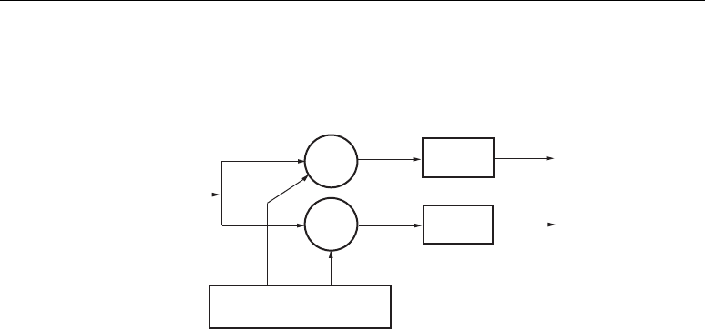
DSP: DESIGNING FOR OPTIMAL RESULTS
30•Xilinx
Some video applications use multi-channel implementations for multiple components of a video
stream. Typical video components are red, green, and blue (RGB) or luma, chroma red, and chroma
blue (YCrCb). The different video components can have the same coefficient sets or different
coefficient sets for each channel by simply changing the coefficient ROM structure.
Creating FIR Filters
Referring to Figure 2-4, Table 2-4, Table 2-5, and Table 2-6, an inner product MAC operation starts
by loading the first operand into the P register. The output of the multiplier is passed through the X
and Y multiplexer, added to zero, and loaded into the P register. Note the load operation OPMODE
with value
0000101 selects zero to be output on the Z multiplexer supplying one of the adder inputs.
A previous MAC inner product can exit via the P bus during this clock cycle.
In subsequent clock cycles, the MAC operation requires the X and Y multiplexers to supply the
multiplier output and the Z multiplexer to supply the output of the P register to the adder. The
OPMODE for this operation, which differs from the load cycle by a single bit, has a value of
0100101.
The description above allows for continuous operation with the previous resulting output and initial
load occurring in the same clock cycle.
Refer to Chapter 4, “MAC FIR Filters,” for detailed information on using DSP48 slices to create
MAC FIR filters.
To create a simple multiply-add processing element using the DSP48 slice shown in Figure 2-4,
set the X and Y multiplexers to multiply and select the cascaded input from another DSP48 output
(PCIN) as the Z MUX input to the arithmetic unit. For a normal multiply-add operation, the
OPMODE value is set to
0010101.
Refer to Chapter 5, “Parallel FIR Filters,” for detailed information on using DSP48 slices to
create Parallel FIR filters.
Figure 2-15: Software-Defined Radio Digital Down Converter
xn() x
I
n() jx
Q
n()+=
UG073_c6_02_070904
v(n)
x
l
(n)
x
Q
(n)
I
Q
M(z)
M(z)
DDS
Direct Digital Synthesizer
×
×

XTREMEDSP DESIGN CONSIDERATIONS
Xilinx • 31
Adder Cascade vs. Adder Tree
In typical direct form FIR filters, an input stream of samples is presented to one data input of separate
multipliers where coefficients supply the other input to the multipliers. An adder tree follows the
multipliers where the outputs from many multipliers are combined as shown in Figure 2-16.
One difficulty of the adder tree concept is defining the size. Filters come in various lengths and
consume a variable number of adders forming an adder tree. Placing a fixed number of adder tree
components in silicon displaces other elements or requires a larger FPGA, thereby increasing the cost
of the design. In addition, the adder tree structure with a fixed number of additions forces the designer
to use logic resources when the fixed number of additions is exceeded. Using logic resources
dramatically reduces performance and increases power consumption. The key to maximizing
Figure 2-16: FIR Filter Adder Tree Using DSP48 Slices
48
48
y(n-6)
18
18
48
48
×
+
+
18
18
18
18
18
18
h0(n)
X(n)
h1(n)
48
48
18
18
48
48
×
+
×
18
18
×
18
18
18
18
h2(n)
X(n)
h3(n)
h4(n)
X(n-2)
X(n-4)
h5(n)
h6(n)
h7(n)
+
+
Z
-2
Z
-2
Z
-2
×
×
×
×
+
The final stages of the post
addition in logic are the
performance bottleneck that
consume more power.
ug073_c1_13_070904
+

DSP: DESIGNING FOR OPTIMAL RESULTS
32•Xilinx
performance and lowering power for DSP math is to remain inside the DSP48 column consisting
entirely of dedicated silicon.
The Virtex-4 solution accomplishes the post-addition process while guaranteeing no wasted
silicon resources. It involves computing the additive result incrementally utilizing a cascaded
approach as illustrated in Figure 2-17. Figure 2-17 is a systolic version of a direct form FIR with a
latency of 10 clocks versus an adder tree latency of six clocks.
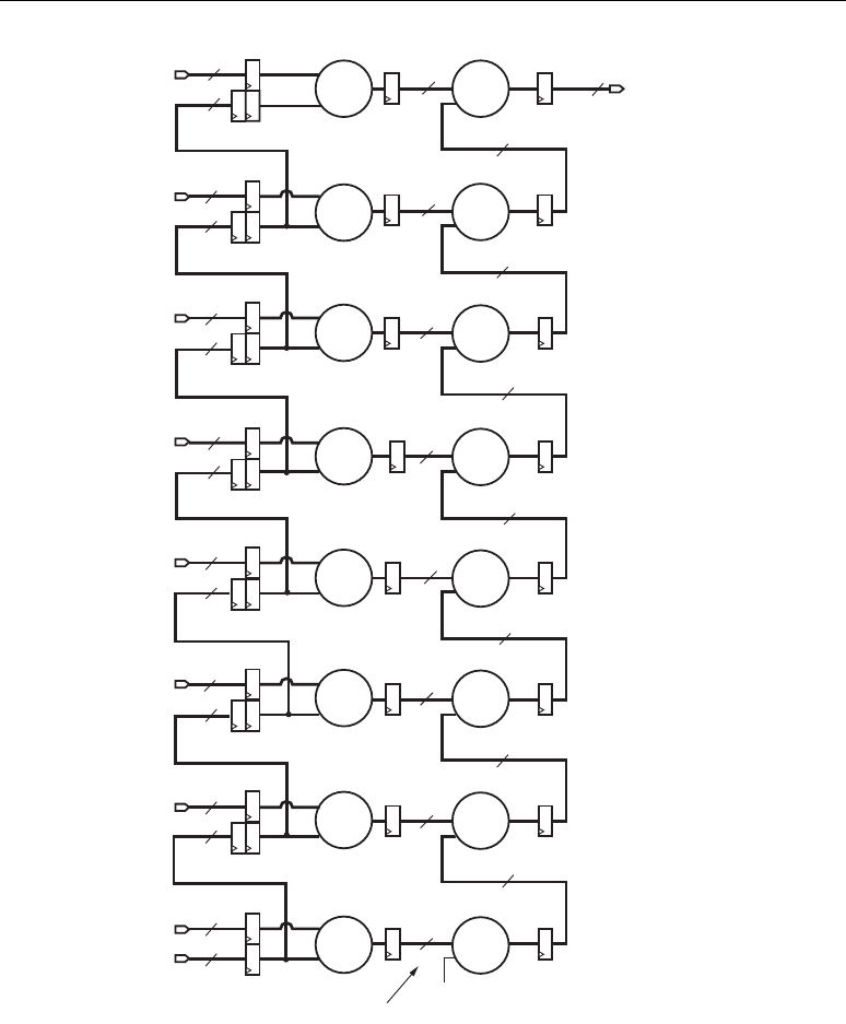
XTREMEDSP DESIGN CONSIDERATIONS
Xilinx • 33
Care should be taken to balance the input sample delay and the coefficients with the cascaded
adder. The adaptive coefficients are staggered in time (wave coefficients).
Figure 2-17: Systolic FIR with Adder Cascade
Slice 7
No wire shift
Slice 8
Slice 6
Slice 5
48
48
48
18
18
48
48
48
48
×
×
+
×
18
18
18
18
×
18
18
48
Y(n–10)
h0(n)
X(n)
h1(n-1)
Slice 3
No wire shift
Slice 4
Slice 2
Slice 1
Zero
48
48
48
18
18
48
48
48
48
×
×
×
18
18
18
18
×
18
18
h2(n-2)
h3(n-3)
h4(n-4)
h5(n-5)
h6(n-6)
h7(n-7)
No wire shift
No wire shift
No wire shift
No wire shift
48
No wire shift
The post adders are
contained wholly in
dedicated silicon for
highest performance
and lowest power
+
+
+
+
+
+
+
Sign extended from 36 bits to 48 bits
ug073_c1_14_070904

DSP: DESIGNING FOR OPTIMAL RESULTS
34•Xilinx
DSP48 Slice Functional Use Models
The use models in this section explain how the DSP48 slices are used in various DSP applications.
Starting with simple multiplication and then growing in complexity, DSP48 slices can be connected
in a variety of ways, trading performance and slice utilization. The tables and use models illustrate a
sampling of different connections.
In some designs full performance is desired and several slices with pipelined registers are used. In
designs with lower sample rates, a single slice is used with multiple clock cycles creating partial
results to be combined at the very end of the computation. Performance choices (i.e., using multiple
clock cycles) can produce efficient slice counts. In either case, the use of pipeline registers allows the
DSP48 slice to run at a very fast, full performance clock rate.
Block diagrams showing the basic connections are also included. The “VHDL and Verilog
Instantiation Templates” section shows how to instantiate and connect the DSP48 slice. In many cases,
starting or ending states are different than the middle states of operation.
Single Slice, Multi-Cycle, Functional Use Models
Table 2-10 lists and summarizes four single slice use models. These examples use the high speed of the
DSP48 slice to accomplish a complicated multi-cycle function by changing the OPMODE bits from
cycle to cycle. Entries in the table name the function with suggestions for DSP48 slice function during
different clock cycles. Further details are in the following subsections. DSP48 designs support extra
pipeline stages to increase overall performance, however, the function remains the same with increased
clock-cycle latency.
Table 2-10: Single Slice DSP48 Implementation
Single Slice
Mode
Slice
Number
Cycle
Inputs
Function and OPMODE[6:0] Output
ABC
35 x 18
Multiply
1 1 0,A[16:0
]
B[17:0] X Multiply 0x05 P[16:0]
2 A[34:17
]
B[17:0] X 17-Bit Shift
Feedback
Multiply Add
0x65 P[52:17]
35 x 35
Multiply
1 1 0,A[16:0
]
0,B[16:0] X Multiply 0x05 P[16:0]
2 A[34:17
]
0,B[16:0] X 17-Bit Shift
Feedback
Multiply Add
0x65
30,A[16:0
]
B[34:17] X Multiply-
Accumulate
0x25 P[33:17]
4 A[34:17
]
B[34:17] X 17-Bit Shift
Feedback
Multiply Add
0x65 P[69:34]

XTREMEDSP DESIGN CONSIDERATIONS
Xilinx • 35
Single Slice, 35 x 18 Multiplier Use Model
The first entry in Table 2-10 indicates how the signed 35 x 18 multiply is designed using a single
DSP48 slice. The 35-bit A and 18-bit B operands are assumed to be signed, two's complement
numbers with results also expressed as a signed, two's complement, 53-bit output. Operand A can
only be 35 bits because when separating an operand into two 18-bit parts, the least-significant part
must have the MSB forced to zero, thereby reducing the available operand bits from 36 to 35.
The multiply function uses one slice (labeled slice 0 in Table 2-10) and computes the final result
in two clocks. The 36-bit, least-significant partial product output formed during the first clock cycle
is computed by multiplying the least-significant 17 bits of Operand A, which are forced positive (sign
bit = 0), with the 18 bits of Operand B (including the original sign).
0,A[16:0] x B[17:0]
The first product is loaded into the output register on this cycle. The lower 17 bits of the first
partial product are the lower 17 bits of the final result. During the second clock cycle, the first partial
product is shifted right by 17 bits, leaving the remaining bits to be fed back and added to the next
partial product. This partial product is formed by multiplying the signed 18-bit Operand B with the
signed upper 18 bits of Operand A. The lower 36 bits of the second partial product are the upper 36
bits of the final result.
A[34:17] x B[17:0]
Figure 2-18 shows the function during both clock cycles for a single DSP48 slice used as a 35-
bit x 18-bit, signed, two's complement multiplier. Increased performance is obtained by using the
pipeline registers before and after the multiplier, however, the clock latency is increased.
Complex
Multiply
11A
Re
[17:
0]
B
Re
[17:0] X Multiply 0x05
2A
Im
[17:
0]
B
Im
[17:0] X Multiply-
Accumulate
0x25 P (Real)
3A
Re
[17:
0]
B
Im
[17:0] X Multiply 0x05
4A
Im
[17:
0]
B
Re
[17:0] X Multiply-
Accumulate
0x25 P
(Imaginary)
Table 2-10: Single Slice DSP48 Implementation (Continued)
Single Slice
Mode
Slice
Number
Cycle
Inputs
Function and OPMODE[6:0] Output
ABC
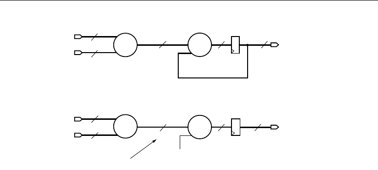
DSP: DESIGNING FOR OPTIMAL RESULTS
36•Xilinx
Single Slice, 35 x 35 Multiplier Use Model
The next entry in Table 2-10 indicates how the signed 35 x 35 multiply is designed using a single
DSP48 slice. The 35-bit A and B operands are assumed to be signed, two's complement numbers with
results expressed as a signed, two's complement, 70-bit output. Operands can only be 35 bits because
when separating an operand into two 18-bit parts. The least-significant 18-bit part must have the
MSB forced to zero, thereby reducing the available operand bits from 36 to 35. The flow is similar to
the 35 x 18 multiply, but instead of two partial products, there are four: a lower partial product, two
middle partial products, and an upper partial product.
The multiply function uses one slice (labeled slice 1 in Table 2-10) and computes the final result
in four clocks. The 36-bit lower partial product formed during the first clock cycle is computed by
multiplying the least-significant 17 bits of Operand A, which are forced positive (sign bit = 0), with
the least-significant 17 bits of Operand B, also forced positive.
0,A[16:0] x 0,B[16:0]
The first product is loaded into the output register on this cycle. All 36-bit products from the
multiplier are sign extended to 48 bits. During the second and third clock cycles, the two middle
products are computed. In clock cycle two, the first or lower partial product in the P register is shifted
right by 17 bits and fed back to the adder/subtracter. The output of the multiplier is the first middle
product, expressed as:
A[34:17] x 0,B[16:0]
The adder/subtracter is set to “add” and the two partial products are added.
In the third clock cycle, the previous result is fed back to the adder/subtracter, but not right
shifted since its bits align with the next computed middle product expressed as:
B[34:17] x 0,A[16:0]
The adder/subtracter is again set to add, and the P register receives the sum of the three partial
products.
Finally, in the fourth clock cycle, the accumulated sum of partial products is again shifted right
by 17 bits, and sign extended leaving the remaining bits to be fed back and added to the next partial
Figure 2-18: Single Slice, 35 x 18-bit Multiplier
0,A[16:0]
PREG = 0,A[16:0] × B[17:0]
B[17:0]
Sign extended from 36 bits to 48 bits
A[34:17]
B[17:0]
A[34:17] × B[17:0]
right “wire shift” by 17 bits
Clock Cycle 2
P = right shifted PREG + (A[34:0] × B[17:0])
P[52:17]
P[16:0]
Zero
48
18
18
48
18
18
48
Clock Cycle 1
48
48
0,A[16:0] × B[17:0]
ug073_c1_15_071004
48
×
×
+
+
XTREMEDSP DESIGN CONSIDERATIONS
Xilinx • 37
product. The upper partial product is formed by multiplying the signed upper 18 bits of B with the
signed upper 18 bits of A.
A[34:17] x B[34:17]
The 70-bit result is output sequentially in 17-bit, 17-bit, and 36-bit segments as shown in
Figure 2-19.
Figure 2-19 shows the function during all four clock cycles for a single DSP48 slice used as a 35-
bit x 35-bit, signed, two's complement multiplier. Increased performance can be obtained by using
the pipeline registers before and after the multiplier, however, the clock latency is increased.
Figure 2-19: Single Slice, 35 x 35-bit Multiplier
0,A[16:0]
PREG = 0,A[16:0] x 0,B[16:0]
0,B[16:0]
A[34:17]
0,B[16:0]
A[34:17] x 0,B[16:0] PREG = right shifted PREG + (A[34:17] x 0,B[16:0])
Sign extended from 36 bits to 48 bits
0,A[16:0]
B[34:17]
0,A[16:0] x B[34:17]
A[34:17]
B[34:17]
A[34:17] x B[34:17]
right “wire shift” by 17 bits
right “wire shift” by 17 bits
Clock Cycle 4
PREG = PREG + (0,A[16:0] x B[34:17])
P = right shifted PREG + (A[34:0] x B[34:17])
P[69:34]
P[33:17]
P[16:0]
Zero
48
18
18
48
18
18
48
48
48
48
18
18
48
48
18
18
48
Clock Cycle 3
Clock Cycle 2
Clock Cycle 1
48
0,A[16:0] x 0,B[16:0]
ug073_c1_16_071004
×
+
×
+
×
+
×
+

DSP: DESIGNING FOR OPTIMAL RESULTS
38•Xilinx
Fully Pipelined Functional Use Models
Table 2-11 summarizes six fully pipelined functional use models. The table provides the function
name and suggests what each DSP48 slice is doing. More details are provided in the following
subsections. The designs are fully pipelined and run at the maximum DSP48 slice clock rate.
Table 2-11: Fully Pipelined DSP48 Implementations
Multiple Slice
Mode
Slice
Inputs
Function and OPMODE[6:0] Output
ABC
35 x 18
Multiply
Figure 2-20
1 0,A[16:0] B[17:0] X Multiply 0x05 P[16:0]
2 A[34:17] B[17:0] X 17-Bit Shifted
Feedback Multiply
Add
0x65 P[52:17]
35 x 35
Multiply
Figure 2-21
1 0,A[16:0] 0,B[16:0] X Multiply 0x05 P[16:0]
2 A[34:17] 0,B[16:0] X 17-Bit Shifted
Feedback Multiply
Add
0x65
3 0,A[16:0] B[34:17] X Multiply Accumulate 0x25 P[33:17]
4 A[34:17] B[34:17] X 17-Bit Shifted
Feedback Multiply
Add
0x65 P[69:34]
18 x 18
Complex
Multiply
Figure 2-22
1A
Re
[17:0] B
Re
[17:0] X Multiply 0x05
2A
Im
[17:0] B
Im
[17:0] X Multiply Accumulate 0x25 P (Real)
3A
Re
[17:0] B
Im
[17:0] X Multiply 0x05
4A
Im
[17:0] B
Re
[17:0] X Multiply Accumulate 0x25 P
(Imaginary)
18 x 18
Complex
MAC
Figure 2-23
1A
Re
[17:0] B
Re
[17:0] X Multiply 0x05
2A
Im
[17:0] B
Im
[17:0] X Multiply Accumulate 0x25 P (Real)
3A
Re
[17:0] B
Im
[17:0] X Multiply 0x05
4A
Im
[17:0] B
Re
[17:0] X Multiply Accumulate 0x25 P
(Imaginary)
35 x 18
Complex
Multiply
Real Part
Figure 2-26
1A
Re
[17:0] B
Re
[17:0] X Multiply 0x05
2A
Im
[17:0] B
Im
[17:0] X Multiply Accumulate 0x25 P (Real)
3A
Re
[17:0] B
Im
[17:0] X Multiply 0x05
4A
Im
[17:0] B
Re
[17:0] X Multiply Accumulate 0x25 P
(Imaginary)
35 x 18
Complex
Multiply
Imaginary
Part
Figure 2-27
1A
Re
[17:0] B
Re
[17:0] X Multiply 0x05
2A
Im
[17:0] B
Im
[17:0] X Multiply Accumulate 0x25 P (Real)
3A
Re
[17:0] B
Im
[17:0] X Multiply 0x05
4A
Im
[17:0] B
Re
[17:0] X Multiply Accumulate 0x25 P
(Imaginary)

XTREMEDSP DESIGN CONSIDERATIONS
Xilinx • 39
Table 2-12 summarizes utilization of more complex digital filters possible using the DSP48. The
small “n” in the Silicon Utilization column indicates the number of DSP48 filter taps. The
construction and operation of complex filters is discussed in Chapter 4, “MAC FIR Filters,” Chapter 5,
“Parallel FIR Filters,” and Chapter 6, “Semi-Parallel FIR Filters.”
Fully Pipelined, 35 x 18 Multiplier Use Model
The previous single slice use models show how performance and power consumption can be traded for
a very small implementation (i.e., single slice). However, many DSP solutions require very high
sample rates. When sample rates approach the maximum inherent clock rate for the math elements in
the FPGA, it becomes necessary to design using parallel, fully pipelined math elements.
With fully pipelined designs, inputs can be presented and an output computed every single clock
cycle. In addition, the DSP48 slice circuits and interconnect are very carefully matched, ensuring no
path becomes the timing bottleneck. Keeping math implementations mostly inside the DSP48
maximizes performance and minimizes power consumption. Of course, pipelining does have increased
clock latency, but this is usually not a problem in DPS algorithms.
In the single slice versions of this algorithm, partial products are computed sequentially and
summed in the adder. For the fully pipelined version of the algorithm, the same partial products are
computed in parallel and summed in the last slice producing a result and consuming new input
operands every clock cycle.
The single slice version of the 35 x 18 multiply uses two clock cycles. In each clock cycle the slice
is presented with different operands, and switching the OPMODE bits modifies the behavior. The
fully pipelined versions connect separate slices with fixed behavior.
In the 35 x 18-bit multiply block diagram (Figure 2-20), the most-significant input data part for
the 35-bit A is delayed with an extra input register in the second slice. This allows the cascading B
input to be available to the second slice multiply at the same time as the most-significant data part for
A. The extra register delay for the cascading B input and most-significant part of A also guarantee the
output of the multiply in the second slice arrive at the same time as the partial product result from the
first slice multiply.
Table 2-12: Composite Digital Filters
Digital Filter Silicon Utilization OPMODE
Multi-Channel FIR n DSP slices, n RAM Static
Direct Form FIR n DSP slices Static
Transposed Form FIR n DSP slices Static
Systolic Form FIR n DSP slices Static
Polyphase Interpolator n DSP slices, n RAM Static
Polyphase Decimator n DSP slices, n RAM Dynamic
CIC Decimation/Interpolation Filters 1 DSP slice per stage Static
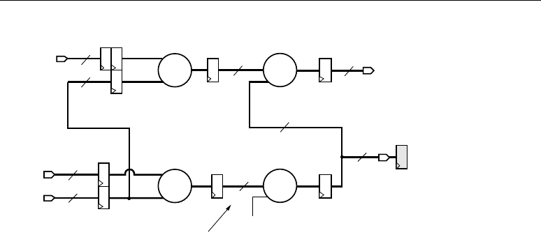
DSP: DESIGNING FOR OPTIMAL RESULTS
40•Xilinx
Fully Pipelined, 35 x 35 Multiplier Use Model
Similar to the 35 x 18-bit example, this fully pipelined design can present inputs every clock cycle. An
output is also computed every single clock cycle. Once again, no particular path becomes the timing
bottleneck. The single slice version of the 35 x 35-bit multiply uses four clock cycles. In each clock
cycle the slice is presented with different operands and switching the OPMODE bits modifies the
behavior. The fully pipelined version connects separate slices with fixed behavior.
In the single slice versions of this algorithm, partial products are computed sequentially and
summed in the adder. For the fully pipelined version of the algorithm, the same partial products are
computed in parallel and summed in the last slice, producing a result and consuming new input
operands every clock cycle.
As in the 35 x 18-bit example, there are additional register stages placed in the input paths to
delay input data until the needed cascading results arrive. In Figure 2-21, the block diagram for the
fully pipelined, 35 x 35 multiply shows where additional input register stages are placed. The
35 x 35-bit multiplier has additional output registers outside of the slice to align the output data. The
notation Z
-3
is in the external register to signify the data must be delayed by three clock cycles. If the
delay is only one cycle, then registers are typically used. When the delay is larger than one, an SRL16
followed by the associated CLB flip-flop achieves maximum design performance.
Figure 2-20: Fully Pipelined, 35 x 18 Multiplier
PREG1[16:0] = 0,A[16:0] × B[17:0]
PREG2 = right shifted PREG1+ (A[34:17] × B[17:0])
0,A[16:0]
B[17:0]
A[34:17]
A[34:17] × B[17:0]
right “wire shift” by 17 bits
Sign extended from 36 bits to 48 bits
0,A[16:0] × B[17:0]
Slice 2
Slice 1
Zero
48
48
48
18
18
18
18
48
48
P[16:0]
P[52:17]
UG073_c1_17_071004
×
+
×
+
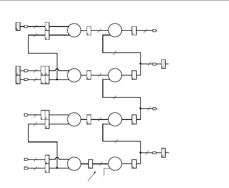
XTREMEDSP DESIGN CONSIDERATIONS
Xilinx • 41
Fully Pipelined, Complex, 18 x 18 Multiplier Use Model
Complex multiplication used in many DSP applications combines operands having both real and
imaginary parts into results with real and imaginary parts. Two operands A and B, each having real
and imaginary parts, are combined as shown in the following equations:
(A_real × B_real) – (A_imaginary × B_imaginary) = P_real
(A_real × B_imaginary) + (A_imaginary × B_real) = P_imaginary
The real and imaginary results use the same slice configuration with the exception of the
adder/subtracter. The adder/subtracter performs subtraction for the real result and addition for the
imaginary result.
Figure 2-22 shows several DSP48 slices used as a complex, 18-bit x 18-bit multiplier.
Figure 2-21: Fully Pipelined, 35 x 35 Multiplier
0,A[16:0]
PREG1 = 0,A[16:0] × 0,B[16:0]
0,B[16:0]
A[34:17]
A[34:17] × 0,B[16:0]
PREG2 = right shifted PREG1 + (A[34:17] × 0,B[16:0])
0,A[16:0]
B[34:17]
0,A[16:0] × B[34:17]
A[34:17]
A[34:17] × B[34:17]
PREG3 = PREG2 + (0,A[16:0] × B[34:17])
PREG4 = right shifted PREG3 + (A[34:0] × B[34:17])
Sign extended from 36 bits to 48 bits
0,A[16:0] × 0,B[16:0]
right “wire shift” by 17 bits
right “wire shift” by 17 bits
Slice 3
Slice 4
Slice 2
Slice 1
Zero
48
48
48
18
18
48
48
48
48
18
18
18
18
18
18
Z
-3
Z
-3
48
48
48
48
P[69:34]
P[33:17]
P[16:0]
ug073_c1_18_071004
×
+
×
+
×
+
×
+
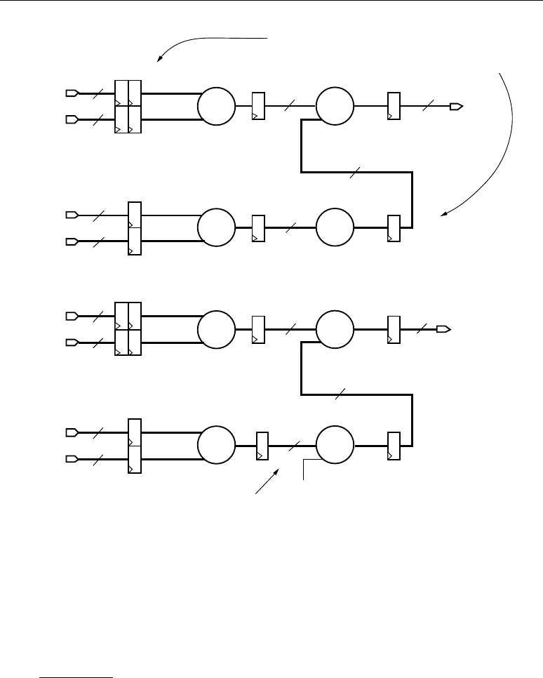
DSP: DESIGNING FOR OPTIMAL RESULTS
42•Xilinx
Note: The real and the imaginary computations are functionally similar using different input
data. The real output subtracts the multiplied terms, and the imaginary output adds the
multiplied terms.
Fully Pipelined, Complex, 18 x 18 MAC Use Model
The differences between complex multiply and complex MAC implementations using several DSP48
slices is illustrated with the next set of equations. As shown, the addition and subtraction of the terms
only occur after the desired number of MAC operations.
For N Cycles:
Slice 1 = (A_real × B_imaginary) accumulation
Slice 2 = (A_imaginary × B_real) accumulation
Slice 3 = (A_real × B_real) accumulation
Slice 4 = (A_imaginary × B_imaginary) accumulation
Figure 2-22: Pipelined, Complex, 18 x 18 Multiply
The two input registers to the left align operands with
the first output register below and avoid fabric.
The benefit is increased performance and lower power.
A_imag
A_real
B_real
B_imag
A_imag
A_real
B_real
B_imag
Slice 3
Slice 4
Slice 2
Slice 1
Sign extended from 36 bits to 48 bits
Zero
48
48
48
18
18
48
48
48
18
18
18
18
18
18
48
48
P_real
P_imag
UG073_c1_19_071004
×
+
×
+
×
+
×
_
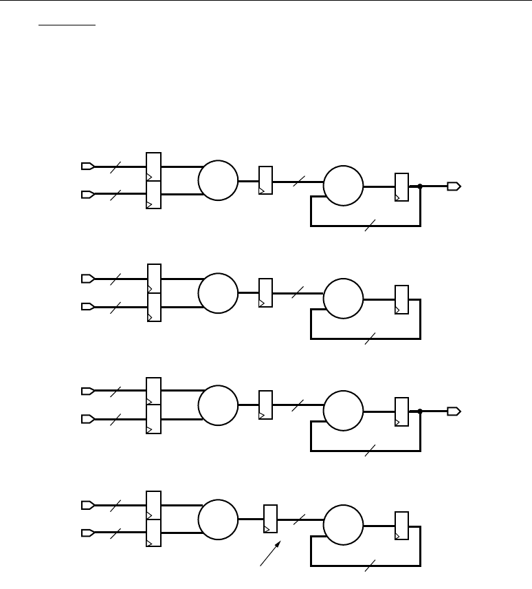
XTREMEDSP DESIGN CONSIDERATIONS
Xilinx • 43
Last Cycle:
Slice 1 + Slice 2 = P_imaginary
Slice 3 – Slice 4 = P_real
During the last cycle, the input data must stall while the final terms are added. To avoid having
to stall the data, instead of using the complex multiply implementation shown in Figure 2-23 and
Figure 2-24, use the complex multiply implementation shown in Figure 2-25.
Figure 2-23: Fully Pipelined, Complex, 18 x 18 MAC (N Cycles)
48
48
18
18
48
48
18
18
18
18
18
18
48
48
48
48
A_imag
P_real
A_real
B_real
B_imag
A_imag
P_imag
A_real
B_real
B_imag
Slice 3
Slice 4
Slice 2
Slice 1
Sign extended from 36 bits to 48 bits
ug073_c1_20_071004
×
+
×
+
×
+
×
+
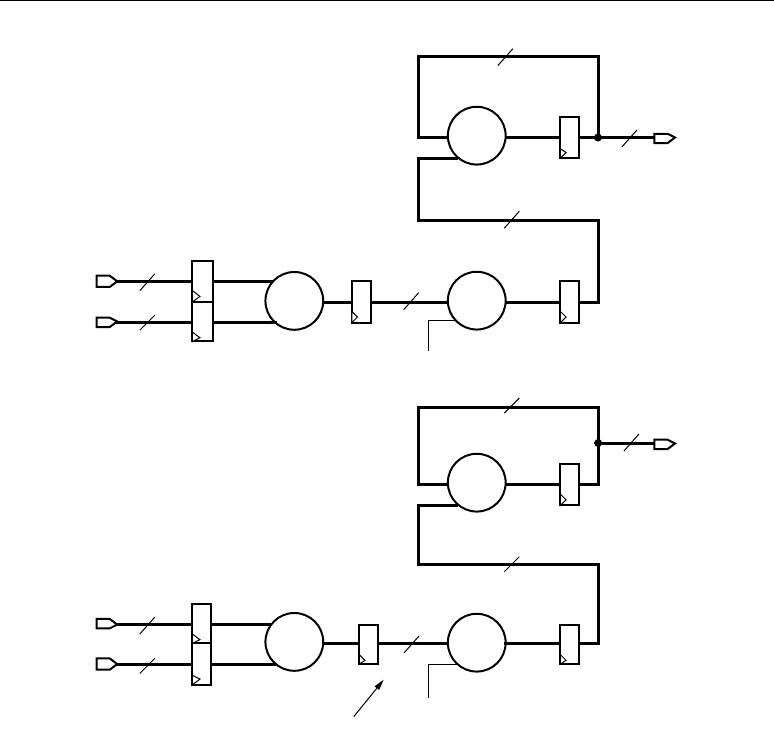
DSP: DESIGNING FOR OPTIMAL RESULTS
44•Xilinx
In Figure 2-24, the N+1 cycle adds the accumulated products, and the input data stalls one cycle.
Figure 2-24: Fully Pipelined, Complex, 18 x 18 MAC (Last or N+1 Cycle)
A_real
B_real
A_real
B_imag
Slice 3
Slice 4
Slice 2
Slice 1
Sign extended from 36 bits to 48 bits
Zero
48
48
48
48
48
18
18
18
18
48
48
48
Zero
P_imag
P_real
ug073_c1_21_070904
+
+
+
+
×
×
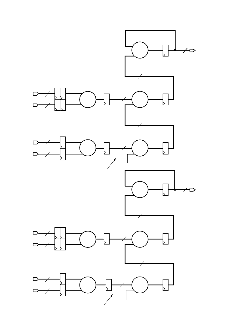
XTREMEDSP DESIGN CONSIDERATIONS
Xilinx • 45
An additional slice used for the accumulation is shown in Figure 2-25. The extra slice prevents
the input data from stalling on the last cycle. The capability of accumulating the P cascade through
the X mux feedback eliminates the pipeline stall.
Figure 2-25: Fully Pipelined, Complex, 18 x 18 MAC with Extra Slice
Zero
48
48
48
18
18
48
48
18
18
18
18
48
48
18
18
48
48
Zero
48
A_imag
A_real
B_real
B_imag
A_imag
A_real
B_real
B_imag
Slice 4
Slice 5
Slice 2
Slice 1
P_imag
P_real
Slice 6
Slice 3
Sign extended from 36 bits to 48 bits
Sign extended from 36 bits to 48 bits
ug073_c1_22_070904
+
×
×
×
×
+
+
+
+
_
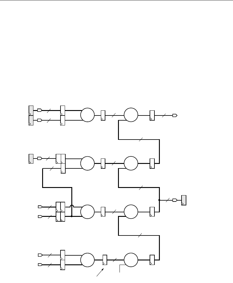
DSP: DESIGNING FOR OPTIMAL RESULTS
46•Xilinx
Fully Pipelined, Complex, 35 x 18 Multiplier Usage Model
Many complex multiply algorithms require higher precision in one of the operands. The equations for
combining the real and imaginary parts in complex multiplication are the same, but the larger
operands must be separated into two parts and combined using partial product techniques. As shown
in the other examples, the real and imaginary results use the same slice configuration with the
exception of the adder/subtracter. The adder/subtracter performs subtraction for the real result and
addition for the imaginary result. The following equations describe the math used to form the real and
imaginary parts for the fully pipelined, complex, 35-bit x 18-bit multiplication.
(A_real × B_real) – (A_imaginary × B_imaginary) = P_real
(A_real × B_imaginary) + (A_imaginary × B_real) = P_imaginary
Figure 2-26 shows the real part of a fully pipelined, complex, 35-bit x 18-bit multiplier.
Figure 2-26: Real Part of a Pipelined, Complex, 35 x 18 Multiply
0,A_imag[16:0]
PREG1 = –(0,A_imag[16:0] × B_imag[17:0])
B_imag[17:0]
0,A_real[16:0]
B_real[17:0]
0,A_real[16:0] × B_real[17:0]
PREG2 = PREG1 + (0,A_real[16:0] × B_real[17:0])
A_real[34:17]
A_real[34:17] × B_real[17:0]
A_imag[34:17]
B_imag[17:0]
A_imag[34:17] × B_imag[17:0]
PREG3 = right shifted PREG2 + (A_real[34:17] × B_real[17:0])
PREG4 = PREG3 – (A_imag[34:17] × B_imag[17:0])
Sign extended from 36 bits to 48 bits
0,A_imag[16:0] × B_imag[17:0]
48
Slice 3
Slice 4
Slice 2
Slice 1
Zero
48
48
18
18
48
48
48
48
Z
–3
Z
–2
Z
–3
18
18
18
18
18
18
48
48
P[16:0]
P[52:17]
Right “wire shift” by 17 bits
ug073_c1_23_071004
×
_
×
_
×
+
×
+
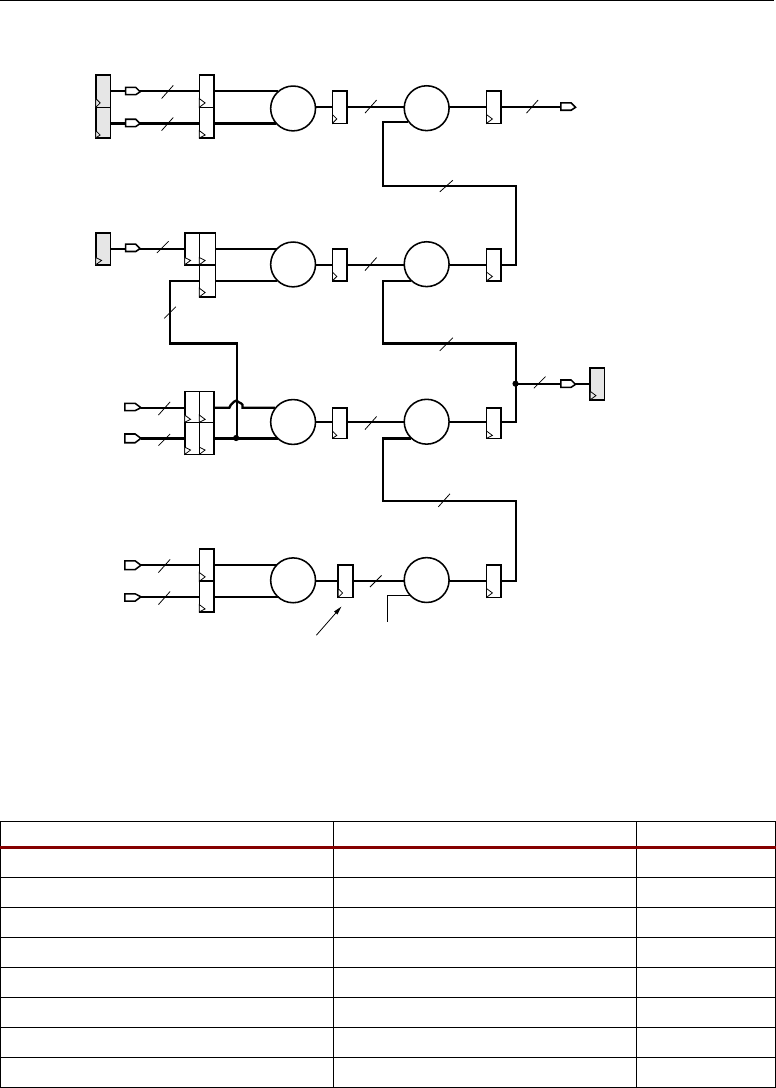
XTREMEDSP DESIGN CONSIDERATIONS
Xilinx • 47
Figure 2-27 shows the imaginary part of a fully pipelined, complex, 35-bit x 18-bit multiplier.
Miscellaneous Functional Use Models
Table 2-13 summarizes a few miscellaneous functional use models.
Figure 2-27: Imaginary Part of a Pipelined, Complex, 35 x 18 Multiply
Table 2-13: Miscellaneous Functional Use Models
Miscellaneous Silicon Utilization OPMODE
18-bit Barrel Shifter
2 DSP slices Static
48-bit Add Subtract
2 DSP slices Static
36-bit Add Subtract Cascade
n DSP slices Static
n word MUX, 48 bit words
2n DSP slices Dynamic
n word MUX, 36 bit words
n DSP slices Dynamic
48-bit Counter
1 DSP slice Static
Magnitude Compare
1 DSP slice, logic Static
Equal to Zero Compare
1 DSP slice, logic Static
0,A_imag[16:0]
PREG1 = (0,A_imag[16:0] × B_real[17:0])
B_real[17:0]
0,A_real[16:0]
B_imag[17:0]
0,A_real[16:0] × B_imag[17:0]
PREG2 = PREG1+ 0,(A_real[16:0] × B_imag[17:0])
A_real[34:17]
A_real[34:17] × B_imag[17:0]
A_imag[34:17]
B_real[17:0]
A_imag[34:17] × B_real[17:0]
PREG3 = right shifted PREG2 + (A_real[34:17] × B_imag[17:0])
PREG4 = PREG3 + (A_imag[34:17] × B_real[17:0])
Sign extended from 36 bits to 48 bits
0,A_imag[16:0] × B_real[17:0]
48
Slice 3
Slice 4
Slice 2
Slice 1
Zero
48
48
18
18
48
48
48
48
18
18
18
18
18
48
48
P[16:0]
P[52:17]
Right “wire shift” by 17 bits
18
ug073_c1_24_071004
Z
–3
Z
–3
Z
–2
×
+
×
+
×
+
×
+
DSP: DESIGNING FOR OPTIMAL RESULTS
48•Xilinx
Dynamic, 18-bit Circular Barrel Shifter Use Model
The barrel shift function is very useful when trying to realign data very quickly. Using two DSP48
slices, an 18-bit circular barrel shifter can be implemented. This implementation shifts 18 bits of data
left by the number of bit positions represented by n. The bits shifted out of the most-significant part
reappear in the lower significant part of the answer completing the circular shift. The equations in
Figure 2-28 describe what value is carried out of the first slice, what this value looks like after shifting
right 17 bits, and finally what is visible as a result.
Figure 2-29 shows the DSP48 used an 18-bit circular barrel shifter. The P register for slice 1
contains leading zeros in the MSBs, followed by the most-significant 17 bits of A, followed by n
trailing zeros. If n equals zero, then are no trailing zeros and the P register contains leading zeros
followed by 17 bits of A.
24 2-input ANDs
1 DSP slice Static
24 2-input XORs
1 DSP slice Static
Up to 48-bit AND
1 DSP slice Static
Figure 2-28: Circular Barrel Shifter Equations
Table 2-13: Miscellaneous Functional Use Models (Continued)
Miscellaneous Silicon Utilization OPMODE
Slice 1, P Carry Out
Slice 2, P Carry In
after 17 bit right shift
Slice 2, P Result
PCOUT[000..., A[17:1], ...000]
A[000..., A[17:17 – N – 1]]
A[000..., A[17 – N:0], A[17:17 – N – 1]]
48 – 18 – N zeros
48 – 18 – N + 17 zeros
48 – 18 – N zeros N MSBs of A
17 bits of A
N MSBs of A
18 – N LSBs of A
N zeros
ug073_c1_25_061304
XTREMEDSP DESIGN CONSIDERATIONS
Xilinx • 49
In the case of n equal to zero (i.e., no shift), the P register of slice 1 is passed to slice 2 with 17 bits
of right shift. This leaves all 48 bits of the P carry input effectively equal to zero since A[17:1] were
shifted toward the least-significant direction. If there is a positive shift amount, then P carry out of
slice 1 contains A[17:1] padded in front by 48 – 17– n zeros and in back by n zeros. After the right
shift by 17, only the n most-significant bits of A remain in the lower 48 bits of the P carry input.
This n-bit guaranteed positive number is added to the A[17:0], left shifted by n bits. In the n
least-significant bits there are zeros. The end result contained in A[17:0] of the second slice P register
is A[17–n:n, 17:17–n+1] or a barrel shifted A[17:0]. The design is fully pipelined and can
generate a new result every clock cycle at the maximum DSP48 clock rate.
A single slice version of the dynamic 18-bit barrel shifter can be implemented. For this
implementation, Table 2-14 describes the DSP48 slice function and OPMODE settings for each clock
cycle.
Figure 2-29: Dynamic 18-Bit Barrel Shifter
Table 2-14: Miscellaneous DSP48 Implementations
Single Slice Mode Cycle
Inputs
Function and OPMODE[6:0] Output
ABC
18-bit Barrel
Shifter
0 A[17:0] B[17:0] X Multiply 0x05
1 A[17:0] B[17:0] X Multiply Accumulate 0x25 P
2 A[17:0] B[17:0] X Multiply 0x05
3 A[17:0] B[17:0] X Multiply Accumulate 0x25 P
Zero
48
48
48
18
18
18
48
A[17:0]
A[0,17:1]
2
n
AR[17:0]
Slice 1
Slice 2
Right “wire shift” by 17 bits
PREG2 = right shifted by 17 PREG1+ n bit left shifted A[17:0]
PREG1 = [000..., 000..., A17:1, ...000]
12 36 – 18 – n + 1 17-bit n
zeros zeros A zeros
ug073_c1_26_071004
×
+
×
+

DSP: DESIGNING FOR OPTIMAL RESULTS
50•Xilinx
VHDL and Verilog Instantiation Templates
This section describes the VHDL and Verilog instantiation templates. In VHDL, each template has a
component declaration section and an architecture section. Insert each part of the template within the
VHDL design file. The port map of the architecture section should include the design signal names.
VHDL Instantiation Template
-- DSP48 : In order to incorporate this function into the
design,
-- VHDL : the following instance declaration needs to be
placed
-- instance : in the body of the design code. The instance name
-- declaration : (DSP48_inst) and/or the port declarations after the
-- code : “=>” declaration maybe changed to properly
reference and
-- : connect this function to the design. All inputs
-- : and outputs must be connected.
-- Library : In addition to adding the instance declaration, a
use
-- declaration : statement for the UNISIM.vcomponents library needs
-- for : to be added before the entity declaration. This
library
-- Xilinx : contains the component declarations for all Xilinx
-- primitives : primitives and points to the models that will be
used
-- : for simulation.
-- Copy the following two statements and paste them before the
-- Entity declaration, unless they already exists.
Library UNISIM;
use UNISIM.vcomponents.all;
-- <-----Cut code below this line and paste into the architecture body---->
-- DSP48: DSP Function Block
-- Virtex-4
-- Xilinx HDL Language Template version 6.1i
DSP48_inst: DSP48 generic map (
AREG => 1, -- Number of pipeline registers on the A input, 0, 1 or 2
BREG => 1, -- Number of pipeline registers on the B input, 0, 1 or 2
B_INPUT => “DIRECT”, -- B input DIRECT from fabric or CASCADE from another
DSP48
CARRYINREG => 1, -- Number of pipeline registers for the CARRYIN input,
0 or 1
CARRYINSELREG => 1, -- Number of pipeline registers for the CARRYINSEL,
0 or 1
CREG => 1, -- Number of pipeline registers on the C input, 0 or 1
LEGACY_MODE => “MULT18X18S”, -- Backward compatibility, NONE,
-- MULT18X18 or MULT18X18S
MREG => 1, -- Number of multiplier pipeline registers, 0 or 1
OPMODEREG => 1, -- Number of pipeline registers on OPMODE input, 0 or 1
PREG => 1, -- Number of pipeline registers on the P output, 0 or 1
SIM_X_INPUT => “GENERATE_X_ONLY”, -- Simulation parameter for
behavior for X on input.
-- Possible values: GENERATE_X,
NONE or WARNING
SUBTRACTREG => 1) -- Number of pipeline registers on the SUBTRACT input,
0 or 1
port map (
BCOUT => BCOUT, -- 18-bit B cascade output

XTREMEDSP DESIGN CONSIDERATIONS
Xilinx • 51
P => P, -- 48-bit product output
PCOUT => PCOUT, -- 38-bit cascade output
A => A, -- 18-bit A data input
B => B, -- 18-bit B data input
BCIN => BCIN, -- 18-bit B cascade input
C => C, -- 48-bit cascade input
CARRYIN => CARRYIN, -- Carry input signal
CARRYINSEL => CARRYINSEL, -- 2-bit carry input select
CEA => CEA, -- A data clock enable input
CEB => CEB, -- B data clock enable input
CEC => CEC, -- C data clock enable input
CECARRYIN => CECARRYIN, -- CARRYIN clock enable input
CECINSUB => CECINSUB, -- CINSUB clock enable input
CECTRL => CECTRL, -- Clock Enable input for CTRL registers
CEM => CEM, -- Clock Enable input for multiplier
registers
CEP => CEP, -- Clock Enable input for P registers
CLK => CLK, -- Clock input
OPMODE => OPMODE, -- 7-bit operation mode input
PCIN => PCIN, -- 48-bit PCIN input
RSTA => RSTA, -- Reset input for A pipeline registers
RSTB => RSTB, -- Reset input for B pipeline registers
RSTC => RSTC, -- Reset input for C pipeline registers
RSTCARRYIN => RSTCARRYIN, -- Reset input for CARRYIN registers
RSTCTRL => RSTCTRL, -- Reset input for CTRL registers
RSTM => RSTM, -- Reset input for multiplier registers
RSTP => RSTP, -- Reset input for P pipeline registers
SUBTRACT => SUBTRACT -- SUBTRACT input
);
-- End of DSP48_inst instantiation
Verilog Instantiation Template
The following is a synthesis instantiation template for the DSP48 slice in Verilog. After the port list
are synthesis attributes with syntax written for the Xilinx Synthesis Tool (XST). If using a different
synthesis tool, consult the tools user guide and change the attributes appropriately. The section after
the synthesis attributes consists of “
defparam” statements that are ignored by the synthesis process,
but are used to initialize the simulation model to match the synthesis attributes during simulation.
// DSP48 : In order to incorporate this function into the design,
// Verilog : the following instance declaration needs to be placed
// instance : in the body of the design code. The instance name
// declaration : (DSP48_inst) and/or the port declarations within the
// code : parenthesis maybe changed to properly reference and
// : connect this function to the design. All inputs
// : and outputs must be connected.
// <-----Cut code below this line---->
// DSP48: DSP Function Block
// Virtex-4
// Xilinx HDL Language Template version 7.1i
DSP48 DSP48_inst (
.BCOUT(BCOUT), // 18-bit B cascade output
.P(P), // 48-bit product output
.PCOUT(PCOUT), // 38-bit cascade output
.A(A), // 18-bit A data input
.B(B), // 18-bit B data input
.BCIN(BCIN), // 18-bit B cascade input
.C(C), // 48-bit cascade input
.CARRYIN(CARRYIN), // Carry input signal
.CARRYINSEL(CARRYINSEL), // 2-bit carry input select
.CEA(CEA), // A data clock enable input

DSP: DESIGNING FOR OPTIMAL RESULTS
52•Xilinx
.CEB(CEB), // B data clock enable input
.CEC(CEC), // C data clock enable input
.CECARRYIN(CECARRYIN), // CARRYIN clock enable input
.CECINSUB(CECINSUB), // CINSUB clock enable input
.CECTRL(CECTRL), // Clock Enable input for CTRL registers
.CEM(CEM), // Clock Enable input for multiplier
registers
.CEP(CEP), // Clock Enable input for P registers
.CLK(CLK), // Clock input
.OPMODE(OPMODE), // 7-bit operation mode input
.PCIN(PCIN), // 48-bit PCIN input
.RSTA(RSTA), // Reset input for A pipeline registers
.RSTB(RSTB), // Reset input for B pipeline registers
.RSTC(RSTC), // Reset input for C pipeline registers
.RSTCARRYIN(RSTCARRYIN), // Reset input for CARRYIN registers
.RSTCTRL(RSTCTRL), // Reset input for CTRL registers
.RSTM(RSTM), // Reset input for multiplier registers
.RSTP(RSTP), // Reset input for P pipeline registers
.SUBTRACT(SUBTRACT) // SUBTRACT input
);
// The following defparams specify the behavior of the DSP48 slice.
// If the instance name to the DSP48 is changed, that change needs to
// be reflected in the defparam statements.
defparam DSP48_inst.AREG = 1; // Number of pipeline registers on the A
input, 0, 1 or 2
defparam DSP48_inst.BREG = 1; // Number of pipeline registers on the B
input, 0, 1 or 2
defparam DSP48_inst.B_INPUT = “DIRECT”; // B input DIRECT from fabric
// or CASCADE from another
DSP48
defparam DSP48_inst.CARRYINREG = 1; // Number of pipeline
registers
// for the CARRYIN input, 0
or 1
defparam DSP48_inst.CARRYINSELREG = 1; // Number of pipeline
registers for the
// CARRYINSEL, 0 or 1
defparam DSP48_inst.CREG = 1; // Number of pipeline registers on the C
input, 0 or 1
defparam DSP48_inst.LEGACY_MODE = “MULT18X18S”; // Backward compatibility,
// NONE, MULT18X18 or
MULT18X18S
defparam DSP48_inst.MREG = 1; // Number of multiplier
pipeline registers, 0 or 1
defparam DSP48_inst.OPMODEREG = 1; // Number of pipeline
registers on
// OPMODE input, 0 or 1
defparam DSP48_inst.PREG = 1; // Number of pipeline registers on the P
output, 0 or 1
defparam DSP48_inst.SIM_X_INPUT = “GENERATE_X_ONLY”; // Simulation
parameter for behavior
// for X on input.
Possible values:
// GENERATE_X, NONE
or WARNING
defparam DSP48_inst.SUBTRACTREG = 1; // Number of pipeline
registers
// on the SUBTRACT input, 0
or 1
// End of DSP48_inst instantiation
Xilinx • 53
Chapter 3
DSP48 Slice Math Functions
The DSP48 slice efficiently performs a wide range of basic math functions, including adders,
subtracters, accumulators, MACs, multiply multiplexers, counters, dividers, square-root functions,
and shifters. The optional pipeline stage within the DSP48 tile ensures high performance arithmetic
functions. The DSP48 column structure and associated routing provides fast routing between DSP48
tiles with less routing congestion to the FPGA fabric. This chapter describes how to use the DSP48
slice to perform some basic arithmetic functions.
Overview
The DSP48 slice is shown in Figure 3-1. Refer to Figure 2-3, page 13 for a diagram showing two
slices cascaded together.
Figure 3-1: DSP Slice Architecture
±
×
ZERO
C
A
B
PCINBCIN
P
18
18
48
1848
18
48 48
48
48
36
48
48
48
Y
X
BCOUT PCOUT
Z
72
18
18
36
36
48
48
Wire Shift Right by 17 Bits
Cascade In from Previous Slice
Cascade Out to Next Slice
ug073_c2_01_061304
SUBTRACT
CIN
DSP: DESIGNING FOR OPTIMAL RESULTS
54•Xilinx
Basic Math Functions
Add/Subtract
The DSP48 slice contains an adder/subtracter unit allowing different combinations of add/subtract
logic to be implemented in a single DSP slice. The output of the DSP48 slice in adder/subtracter mode
is:
Output = Z ± (X + Y +CIN)
The X, Y, and Z terms in this equation refer to the X, Y, and Z multiplexers shown in Figure 3-1.
The inputs to the X, Y, and Z multiplexers are routed to the outputs using OPMODE settings as
shown in Table 3-1. The CIN term is the Carry Input to the Adder/subtracter unit.
Determining whether an addition or a subtraction (±) takes place is controlled by the
SUBTRACT input to the adder/subtracter unit. The SUBTRACT input must be set to 0 to add, and
1 to subtract.
The Verilog code for this 48-bit adder is in the reference design file:
ADDSUB48.v, and the
VHDL code is in the reference design file:
ADDSUB48.vdh. This code can be used to implement any
data combination for this equation by using the different OPMODEs found in Table 3-1.
Accumulate
A DSP48 slice can implement add and accumulate functions with up to 36-bit inputs. The output
equation of the accumulator is:
Output = Output + A:B + C
Concatenate (:) the A and B inputs to provide a 36-bit input from Multiplexer X using the
setting OPMODE[1:0] =
0’b11. Select the C input to Multiplexer Y using the setting
OPMODE[3:2] =
0’b11. To add (accumulate) the output of the slice, select the feedback path (P)
through the Z multiplexer using the setting OPMODE[6:4] =
0’b010.
Other accumulate functions can be implemented by changing the OPMODE selection for the Z
input multiplexer. To get an output of:
Output = Shift(P) ± (A:B + C)
Table 3-1: OPMODE Settings for the Z, Y, and X Multiplexers
Z OPMODE[6:4] Y OPMODE[3:2] X OPMODE[1:0]
0 000 0 00 0 00
PCin 001 AxB 01 AxB 01
P 010 Illegal 10 P 10
C 011 C 11 A:B 11
ShiftPCin 101
ShiftP 110
Notes:
1. If one of X or Y is set to 01, the other one must also be set to 01.
2. For Carryin Select (CIN) see “Carry Input Logic” in Chapter 2.

DSP48 SLICE MATH FUNCTIONS
Xilinx • 55
use the setting OPMODE[6:4] =
0’b110 to select the Shift(P) input to the Z multiplexer. To get
an output of:
Output = 0 ± (A:B +C)
(no accumulation) use the setting OPMODE [6:4] =
0’b0000 to select the ZERO input to the
Z multiplexer.
The Verilog code for the accumulator is in the reference design file
ACCUM48.v, and the VHDL
code is in the reference design file
ACCUM48.vhd.
Multiply Accumulate (MAC)
The DSP48 slice allows two 18-bit numbers to be multiplied together, and the product to be added to
or subtracted from a previous product, a “0”, or a shifted product. In addition, rounding of any of the
add, subtract, previous product, 0, or shifted product options is also possible.
The input added or subtracted from the product is from the output of the Z multiplexer. This
output is set using the corresponding OPMODE setting as shown in Table 3-1. Cascade the MAC tree
by selecting the PCIN signal from the previous slice as the output from the Z multiplexer.
The Verilog code for the multiply-accumulate function is in the reference design file
MAC.v, and
the VHDL code is in the reference design file
MAC.vhd.
Multiplexer
There are three multiplexers in a DSP48 slice: the 3:1 Y multiplexer, the 4:1 X multiplexer, and the
6:1 Z multiplexer. Only one multiplexer is active to use the slice as a pure multiplexer. Make the other
two multiplexers inactive by choosing the OPMODE selecting the ZERO inputs. The two DSP48
tiles in a slice can be combined to make wider input multiplexers.
Barrel Shifter
An 18-bit barrel shifter can be implemented using the two DSP48 tiles in the DSP slice. To barrel
shift the 18-bit number A[17:0] two positions to the left, the output from the barrel shifter is
A[15:0], A[17], and A[16]. This operation is implemented as follows.
The first DSP48 is used to multiply {0,A[17:1]} by 2
2
. The output of this DSP48 tile is now
{0,A[17:1],0,0}. The output from the first tile is fed into the second DSP48 tile over the
PCIN/PCOUT signals, and is passed through the 17-bit right-shifted input. The input to the Z
multiplexer becomes {0,A[17],A[16]}, or {0,A[17:0],0,0} shifted right by 17 bits.
The multiplier inputs to the second DSP48 tile are A = A[17:0] and B = 2
2
. The output of this
multiplier is {A[17:0], 0,0}. This output is added to the 17-bit right-shifted value of {0,A[17],A[16]}
coming from the previous slice. The 18-bit output of the adder is {A[15:0],A[17],A[16]}. This is the
initial A input shifted by two to the left.
The Verilog code is in the reference design file
barrelshifter_18bit.v, and the VHDL code
is in the reference design file
barrelshifter_18bit.vhd).
Counter
The DSP48 slice can be used as a counter to count up by one on each clock cycle. Setting the
SUBTRACT input to ‘0’, the carry-in input (CIN) to ‘1’, and OPMODE [6:0] =
0’b0100000 gives
an output of P + CIN. After the first clock, the output P is 0 + 1 = 1. Subsequent outputs are P + 1.

DSP: DESIGNING FOR OPTIMAL RESULTS
56•Xilinx
This method is equivalent to counting up by one. The counter can be used as a down counter by
setting the SUBTRACT input to a ‘1’ at the start.
The counter can also be preloaded using the C input to provide the preload value. Setting the
Carry In input (CIN) to ‘1’ and OPMODE [6:4] =
0’b0110000 gives an output of P = C+1 in the
first cycle. For subsequent clocks, set the OPMODE to select P = P+1 by changing OPMODE [6:4]
from
0’b0110000 to 0’b0100000.
The Verilog code for a loadable counter is in the reference design file
CNTR_LOAD.v, and the
VHDL code for a loadable counter is in the reference design file
CNTR_LOAD.vhd.
Multiply
A single DSP48 slice can implement an 18x18 signed or unsigned multiplier. Larger multipliers can
be implemented in a single DSP48 slice by sequentially shifting the appropriate number of bits in
each clock cycle. The Verilog implementation of an 18x18 multiplier is in the reference design file
MULT18X18_PARALLEL.v, and the VHDL implementation is in the reference design file
MULT18X18_PARALLEL.vhd.
The Verilog implementation of a 35x35 multiplier and a sequential 35x35 multiplier are in the
reference design files
MULT35X35_PIPE.v and MULT35X35_SEQUENTIAL_PIPE.v respectively.
The VHDL implementation of a 35x35 multiplier and a sequential 35x35 multiplier are in the
reference design files
MULT35X35_PIPE.vhd and MULT35x35_SEQUENTIAL_PIPE.vhd,
respectively.
Divide
Binary division can be implemented in the DSP48 slice by performing a shift and subtract or a
multiply and subtract. The DSP48 slice includes a shifter, a multiplier, and adder/subtracter unit to
implement binary division. The division by subtraction and division by multiplication algorithms are
shown below. These algorithms assume:
1. N > D
2. N and D are both positive
If either N or D is negative, use the same algorithms by taking the absolute positive values for N
and D and making the appropriate sign change in the result.
The terms N and D in the algorithms refer to the number to be divided (N) and the divisor (D).
The terms Q and R in the algorithms refer to the quotient and remainder, respectively.
Dividing with Subtraction
The shift and subtract algorithm can be explained as follows:
If N is an 8-bit integer and D is not more than 8 bits wide, N/D = Q + R
1. Assign the 8-bit register R the value “
00000000”.
2. Shift the R register one bit to the left and fill in the LSB with N[8-n].
3. Calculate R-D.
4. Set R and set Q:
a. If R-D is positive, set Q[8-n] to 1 and R = R-D
b. If R-D is negative, set Q[0] to 0 and R = R
5. Repeat Steps 2 to 4, filling in R[n] each time with N[8-n], where n is the number of the
iteration. Q[8-n] is filled each time in Step 4.

DSP48 SLICE MATH FUNCTIONS
Xilinx • 57
After the eighth iteration, Q[7:0] contains the quotient, and R[7:0] contains the remainder. For
example:
Step
Iteration
(n)
Action
After Action
QR
1 1 R = 0000,0000 xxxx,xxxx 0000,0000
2 1 R <-- N[7] = 0000,0000 xxxx,xxxx 0000,0000
3 1 R-D = Negative xxxx,xxxx 0000,0000
4 1 Q[7] = 0 0xxx,xxxx 0000,0000
2 2 R <-- N[6] = 0000,0000 0xxx,xxxx 0000,0000
3 2 R-D = Negative 0xxx,xxxx 0000,0000
4 2 Q[6] = 0 00xx,xxxx 0000,0000
2 3 R <-- N[5] = 0000,0000 00xx,xxxx 0000,0000
3 3 R-D = Negative 00xx,xxxx 0000,0000
4 3 Q[5] = 0 000x,xxxx 0000,0000
2 4 R <-- N[4] = 0000,0000 000x,xxxx 0000,0000
3 4 R-D = Negative 000x,xxxx 0000,0000
4 4 Q[4] = 0 0000,xxxx 0000,0000
2 5 R <-- N[3] = 0000,0001 0000,xxxx 0000,0001
3 5 R-D = Negative 0000,xxxx 0000,0001
4 5 Q[3] = 0 0000,0xxx 0000,0001
2 6 R <-- N[2] = 0000,0010 0000,0xxx 0000,0010
3 6 R-D = Negative 0000,0xxx 0000,0010
4 6 Q[2] = 0 0000,00xx 0000,0010
2 7 R <-- N[1] = 0000,0100 0000,00xx 0000,0100
3 7 R-D = Positive 0000,00xx 0000,0100
4 7 Q[1] = 1, R = 0000,0001 0000,001x 0000,0001
2 8 R <-- N[0] = 0000,0010 0000,001x 0000,0010
3 8 R-D = Negative 0000,001x 0000,0010
8 Q[2] = 0 0000,0010 0000,0010
N
D
-----
8
3
-----
0000 1000,
011
------------------------------------------------ Q(10) R(10)+== =

DSP: DESIGNING FOR OPTIMAL RESULTS
58•Xilinx
Dividing with Multiplication
The multiply and subtract method consists of rewriting N/D = Q + R as N= D * (Q + R).
The answer is calculated using the following steps for an 8-bit N/D:
1. Set the initial value of Q[8-n] =1 and the bits right of Q[8-n] to 0.
2. Calculate D*Q.
3. Calculate N- (D*Q).
a. If step 2 is positive, N > (D*Q), set Q[8-n] to a ‘1’.
b. If step 2 is negative, N < (D*Q), set Q[8-n] to a ‘0’.
4. Repeat steps 1 to 3.
After the eighth iteration, Q[7:0] contains the quotient and N - (D*Q) contains the remainder.
Using the same example:
Step
Iteration
(n)
Action
After Action
Q
1 1 Q[8-1] = 1, Set the bits right of Q[8-1] to 0 1000,0000
2 1 D*Q = 3 * 128 = 384 1000,0000
3 1 N - (D*Q) = 8 - 384 = Negative Q[8-1] = 0 0000,0000
1 2 Q[8-2] = 1, Set the bits right of Q[8-2] to 0 0100,0000
2 2 D*Q = 3 * 64 = 192 0100,0000
3 2 N - (D*Q) = 8 - 192 = Negative Q[8-2] = 0 0000,0000
1 3 Q[8-3] = 1, Set the bits right of Q[8-3] to 0 0010,0000
2 3 D*Q = 3 * 32 = 96 0010,0000
3 3 N - (D*Q) = 8 - 96 = Negative Q[8-3] = 0 0000,0000
1 4 Q[8-4] = 1, Set the bits right of Q[8-4] to 0 0001,0000
2 4 D*Q = 3 * 16 = 48 0001,0000
3 4 N - (D*Q) = 8 - 48 = Negative Q[8-4] = 0 0000,0000
1 5 Q[8-5] = 1, Set the bits right of Q[8-5] to 0 0000,1000
2 5 D*Q = 3 * 8 = 24 0000,1000
3 5 N - (D*Q) = 8 - 24 = Negative Q[8-5] = 0 0000,0000
1 6 Q[8-6] = 1, Set the bits right of Q[8-6] to 0 0000,0100
2 6 D*Q = 3 * 4 = 12 0000,0100
3 6 N - (D*Q) = 8 - 12 = Negative Q[8-6] = 0 0000,0000
1 7 Q[8-7] = 1, Set the bits right of Q[8-7] to 0 0000,0010
2 7 D*Q = 3 * 2 = 6 0000,0010
3 7 N - (D*Q) = 8 - 6 = Positive
Q[8-7] = 1
0000,0010
8
3
-----
0000 1000,
011
------------------------------------------------ Q(10) R(10)+==
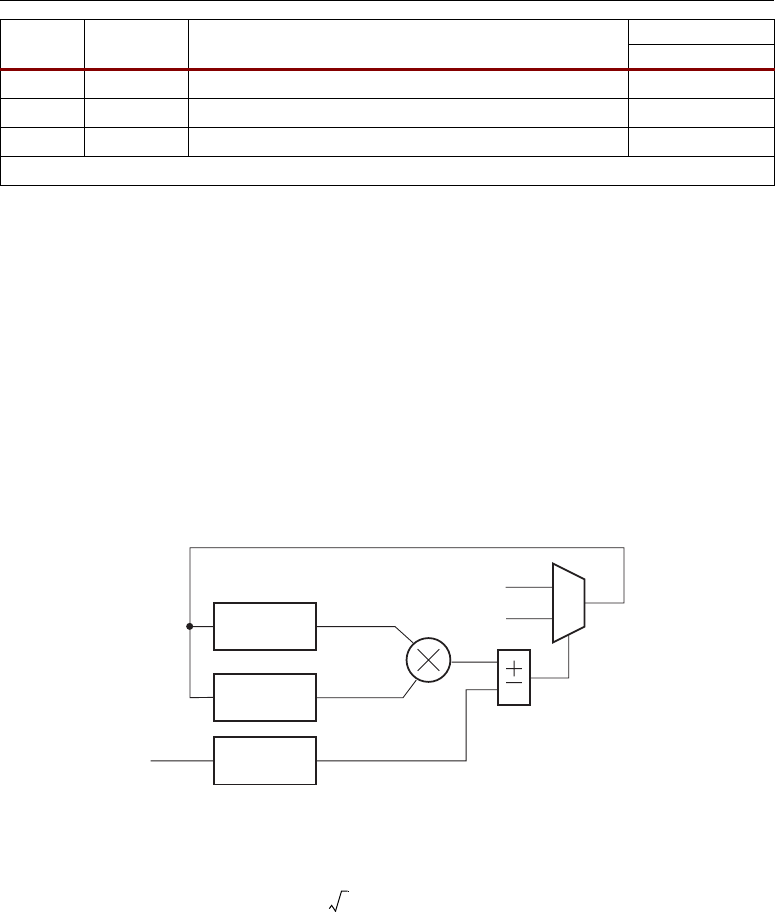
DSP48 SLICE MATH FUNCTIONS
Xilinx • 59
Both of the division implementations are possible in one DSP48 slice. The slice usage for 8-bit
division is one DSP48, and the latency is eight clock cycles.
The Verilog code for the Divide by Subtraction implementation is in the reference design file
DIV_SUB.v, and the VHDL code is in the reference design file DIV_SUB.vhd. The Verilog code for
the Divide by Multiplication implementation is in
DIV_MULT.v and the VHDL code for the second
implementation is in
DIV_MULT.vhd.
Square Root
The square root of an integer number can be calculated by successive multiplication and subtraction.
This is similar to the subtraction method used to divide two numbers. The square root of an N-bit
number will have N/2 (rounded up) bits. If the square root is a fractional number, N/2 clocks are
needed for the integer part of the answer, and every following clock gives one bit of the fraction part.
The logic needed to compute this is shown in Figure 3-2.
The square root for an 8-bit number can be calculated as follows:
Y is the integer part of the root, and Z is the fraction part. Register A refers to the registers found
on the A input to the DSP48 slice, and Register C refers to the registers found on the C input to the
DSP48 slice
1. Read the number into Register C. Set Register A to
8’b10000000.
2. Calculate Register C – (Register A * Register A).
3. If step 2 is positive, set Register A[(8-clock)] = 1,
Register A[(8-clock)-1] = 1
1 8 Q[8-8] = 1 0000, 0011
2 8 D*Q = 3 * 3 = 9 0000,0011
3 8 N - (D*Q) = 8 – 9 = Negative Q[8-8] = 0 0000,0010
Remainder = N-(D*Q) = 8-(3*2) = 2
Figure 3-2: Square Root Logic
Step
Iteration
(n)
Action
After Action
Q
Register
A
Register
A
Input = Reg C
Multiplier
Subtractor
1'b1
1'b0
Input
UG073_c2_02_061304
XY.Z=

DSP: DESIGNING FOR OPTIMAL RESULTS
60•Xilinx
If step 2 is negative, set Register A[(8-clock)] = 0,
Register A[(8-clock)-1] = 1
4. Repeat steps 1 to 3.
Four clocks are required to calculate the integer part of the value (Y). The number of clocks
required for the fraction part (Z) depends on the precision required. For an 8-bit input value, the value
in Reg_A after eight clocks includes the integer part given by the four MSBs and the fractional part
given by the four LSBs.
For example, find the square root of
11 decimal = 3.3166. Because 11 decimal is a 4-bit binary
number, the integer part is two bits wide and is obtained in two clock cycles. The bit width of the
fractional part depends on the precision required. In this example, four bits of precision are used
requiring four clock cycles.
The binary of value of 11 decimal is
1011. Expressed as an 8-bit number, it becomes
0000,1011. Store this value as 0000,1011,0000,0000. The last eight bits are necessary because
the result is an 8-bit number, and 8 bits * 8 bits gives a 16-bit multiplication result.
Clock Step Action
1 1 Register A = 1000,0000
1 2 0000,1011,0000,0000 – (1000,0000 * 1000,0000)
1 3 Step 2 is negative. Set Register A to 0100,0000
2 1 Register A = 0100,0000
2 2 0000,1011,0000,0000 – (0100,0000 * 0100,0000)
2 3 Step 2 is negative. Set Register A to 0010,0000
3 1 Register A = 0010,0000
3 2 0000,1011,0000,0000 – (0010,0000 * 0010,0000)
3 3 Step 2 is positive. Set Register A to 0011,0000
4 1 Register A = 0011,0000
4 2 0000,1011,0000,0000 – (0011,0000* 0011,0000)
4 3 Step 2 is positive. Set Register A to 0011,1000
5 1 Register A = 0011,1000
5 2 0000,1011,0000,0000 – (0011,1000* 0011,1000)
5 3 Step 2 is negative. Set Register A to 0011,0100
6 1 Register A = 0011,0100
6 2 0000,1011,0000,0000 – (0011,0100* 0011,0100)
63
Step 2 is positive. Set Register A to 0011,0110
7 1 Register A = 0011,0110
7 2 0000,1011,0000,0000 – (0011,0110* 0011,0110)
7 3 Step 2 is negative. Set Register A to 0011,0101
8 1 Register A = 0011,0101
DSP48 SLICE MATH FUNCTIONS
Xilinx • 61
The output is in Register A and is
0011,0101. The final answer is 11.0101.
The Verilog code for this implementation (8-bit input, 8 clocks) is in
SQRT.v, and the VHDL
code is in
SQRT.vhd.
Square Root of the Sum of Squares
The sum of squares is a widely used DSP function. The sum of squares can be either of the forms listed
in Equation 3-1 or Equation 3-2.
Equation 3-1
Equation 3-2
These functions are basic multiply-accumulate operations easily implemented on the DSP48 slice
as described in “Multiply Accumulate (MAC),” page 55. A variation of this function is when the
square root of either of the above equations is needed. In this case, the OPMODE does the MAC
function for n cycles and then switches to do the square root function for the next n cycles. The
Subtract input is dynamic and does an “add” for the MAC cycles and a “subtract” for the square root
cycles.
With the SUBTRACT input equal to 0, the OPMODE for the function is
0110101. A square
root function is implemented by changing the SUBTRACT input to a “1”.
8 2 0000,1011,0000,0000 – (0011,0101* 0011,0101)
8 3 Step 2 is positive.
Clock Step Action
SoS A
2
B
2
+=
SoS Ai
2
i 0=
In1–=
∑
=
or
SoS A
2
B
2
+=
SoS Ai
2
i0=
In1–=
∑
=
or

DSP: DESIGNING FOR OPTIMAL RESULTS
62•Xilinx
Conclusion
The DSP48 slice has a variety of features for fast and easy implementation of many basic math
functions. The dedicated routing region around the DSP48 slice and the feedback paths provided in
each slice result routing improvements. The high-speed multiplier and adder/subtracter unit in the
slice delivers high-speed math functions.

Xilinx • 63
Chapter 4
MAC FIR Filters
This chapter describes the implementation of a Multiply-Accumulate (MAC) Finite Impulse Response
(FIR) filter using the DSP48 slice in a Virtex™-4 device. Because the Virtex-4 architecture is flexible,
constructing FIR filters for specific application requirements is practical. Creating optimized filter
structures of a sequential nature saves resources and potential clock cycles.
This chapter demonstrates two sequential filter architectures: the single-multiplier and the dual-
multiplier MAC FIR filter. Reference design files are available for the System Generator in DSP,
VHDL, and Verilog. These reference designs permit filter parameter changes including coefficients
and the number of taps.
Overview
A large array of filtering techniques is available to signal processing engineers. A common filter
implementation uses the single multiplier MAC FIR filter. In the past, this structure used the
Virtex-II embedded multipliers and 18K block RAMs. The Virtex- 4 DSP48 slice contains higher
performance multiplication and arithmetic capabilities specifically designed to enhance the use of
MAC FIR filters in FPGA-based Digital Signal Processing (DSP).
Single-Multiplier MAC FIR Filter
The single-multiplier MAC FIR is one of the simplest DSP filter structures. The MAC structure uses
a single multiplier with an accumulator to implement a FIR filter sequentially versus a full parallel
FIR filter. This trade-off reduces hardware by a factor of N, but also reduces filter throughput by the
same factor. The general FIR filter equation is a summation of products (also know as an inner
product), defined as:
Equation 4-1
In this equation, a set of N coefficients is multiplied by N respective data samples, and the inner
products are summed together to form an individual result. The values of the coefficients determine
the characteristics of the filter (e.g., low-pass filter, band-pass filter, high-pass filter). The equation can
be mapped to many different implementations (e.g., sequential, semi-parallel, or parallel) in the
different available architectures.
y
n
x
ni–
h
i
i0=
N1–
∑
=
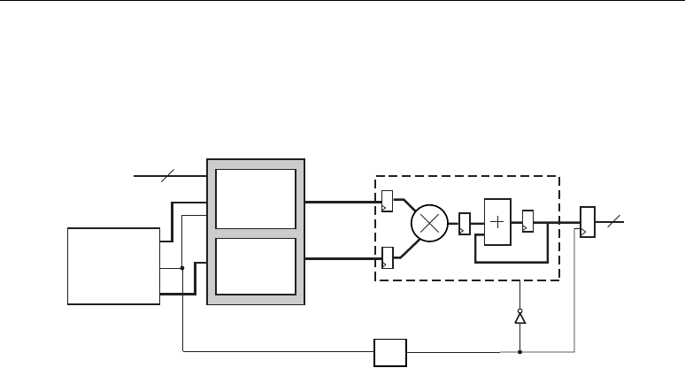
DSP: DESIGNING FOR OPTIMAL RESULTS
64•Xilinx
For slow sample rate requirements and a large number of coefficients, the single MAC FIR filter
is well suited and dual-port block RAM is the optimal choice for the memory buffer. This structure is
illustrated in Figure 4-1. If the number of coefficients is small, distributed memory and the SRL16E
can be used as the data and coefficient buffers. For more information on using distributed memory,
refer to “Using Distributed RAM for Data and Coefficient Buffers,” page 70.
The input data buffer is implemented in dual-port block RAM. The read address port is clocked
N times faster than the input samples are written into the data port, where N is the number of filter
taps. The filter coefficients are also stored in the same dual-port block RAM, and are output at port B.
Hence, the RAM is used in a mixed-mode configuration. The data is written and read from port A
(RAM mode), and the coefficients are read only from port B (ROM mode).
The control logic provides the necessary address logic for the dual-port block RAM and creates a
cyclic RAM buffer for port A (data buffer) to create the FIR filter delay line. An optional output
capture register maybe required for streaming operation, if the accumulation result can not be
immediately used in downstream processing.
The multiplier followed by the accumulator sums the products over the same number of cycles as
there are coefficients. With this relationship, the performance of the MAC FIR filter is calculated by
the following equation:
Maximum Input Sample Rate = Clock Speed / Number of Taps Equation 4-2
If the coefficients possess a symmetric shape, a slightly costlier structure is available (see
“Symmetric MAC FIR Filter,” page 72), however, the maximum sampled rate is doubled. The sample
rate of the costlier structure is defined as follows:
Sample Rate = Clock Speed / (1/2 x number of taps) Equation 4-3
Figure 4-1: Single-Multiplier MAC FIR Filter
Data Samples
96 x 18
Coefficients
96 x 18
Control
Data Addr
WE
Dual-Port Block RAM
Optional Output
Register Used
18
Coef Addr
18
A
B
load
P
Z
-4
DSP48 Slice
OPMODE = 0100101
UG073_c3_02_081804

MAC FIR FILTERS
Xilinx • 65
Bit Growth
The nature of the FIR filter, with numerous multiplies and adds, outputs a larger number of bits from
the filter than are present on the filter’s input. This effect is the "bit growth" or the "gain" of a filter.
These larger results cannot be maintained throughout a system due to cost implications. Therefore, the
full precision result is typically rounded and quantized (refer to “Rounding,” page 69) back to a
desired level. However, it is important to calculate the full precision output in order to select the
correct bits from the output of the MAC.
A simple explanation for implementation purposes involves considering the maximum value
expected at the output (saturation level). A greater understanding of the specific filter enhances the
accuracy of the output bit width. The following two techniques help determine the full precision
output bit width.
Generic Saturation Level
This technique assumes every value in the filter could be the worst possible for the size of the two’s
complement numbers specified. Using the generic saturation level is a good starting point when the
coefficients are unknown, but the number of bits required to represent them is known. For example,
if the coefficients are reloadable, as in adaptive filters.
Output Width = ceil (log2 (2
(b-1)
x 2
(c-1)
x N) + 1 Equation 4-4
where:
ceil: Rounds up to the nearest integer
b: Number of bits in the data samples
c: Number of bits in the coefficients
Coefficient Specific Saturation Level
This technique uses the magnitude-only sum of actual coefficient values and applies the worst-case
data samples to the filter. More accurate calculations could be required if a bit maximum is reached.
With actual coefficients, the output for the worst possible inputs can be determined.
Output Width = ceil (log2 (2
(b-1)
x abs (sum (coef)) x N) + 1 Equation 4-5
where:
ceil: Rounds up to the nearest integer
abs: Makes the absolute value of a number (not negative)
sum: Sums all the values in an array
B: Number of bits in the data samples
C: Number of bits in the coefficients
If the output width exceeds 48 bits, there are notable effects on the size (in terms of the number
of DSP48 slices used to implement the filter), because the DSP48 slice is limited to a 48-bit result.
The output width can be extended by using more DSP48 slices, however, reconsidering the
specification is more practical.
Control Logic
The control logic is very straightforward when using an SRL16E for the data buffer. For dual-port
block RAM implementations the cyclic RAM buffer is required. This can complicate the control
logic, and there are two different ways this control can be implemented. Both techniques produce the
same results, but one way uses all slice-based logic to produce the results, while the other way embeds
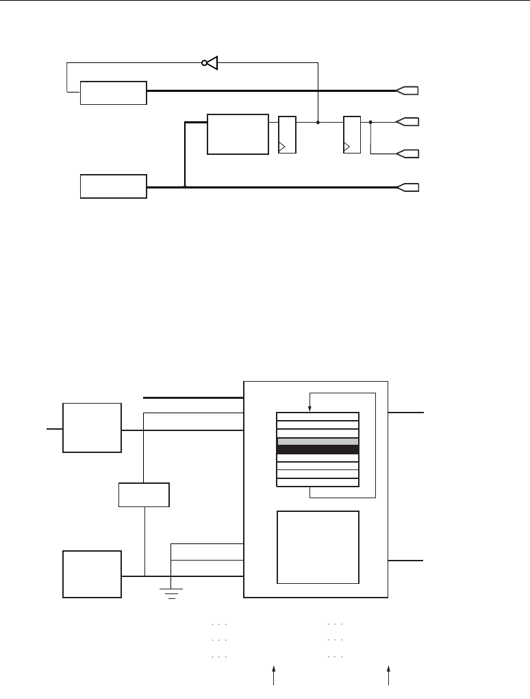
DSP: DESIGNING FOR OPTIMAL RESULTS
66•Xilinx
the control in the available space in the Block RAM. The basic architecture of the control logic for the
slice based approach is outlined in Figure 4-2.
The control logic consists of two counters. One counter drives the address of the coefficient
section of the dual-port block RAM, while the other controls the address for the data buffer. A
comparator controls an enable to the data buffer counter to disable the count for one cycle every output
sample, and writes a new sample into the data buffer every N cycles. A simplified diagram of the
control logic and the memory is shown in Figure 4-3.
Figure 4-2: Dual-Port Block RAM MAC FIR Filter Control Logic Using Slices
Figure 4-3: Control Logic and Memory
Coefficient
Counter
Coefficient
Address
Load ACC
Data
Counter
WE
Data
Address
en addr
en
addr
A = 2N – 2
UG073_c3_03_090204
Counter
N – (2N–1)
Counter
0 – (N–1)
A = 2N–2
D
IN
A
D
IN
B
WE
data addr
WE
coef addr
addr
addren
D
OUT
A
D
OUT
B
RAM must be:
Read after Write
Coefficient
ROM
Dual-Port RAM
DIN D1 X X X
Data Addr
Coeff Addr
XX XD2 X X X X D3 X X X
0 1 2 3 94 95 93 9495 2100194 95
96 97 98 99 190 191 96 9897 99 190191 96 9897 99
WE WE
UG073_c3_04_090204

MAC FIR FILTERS
Xilinx • 67
The cyclic data RAM buffer is required to emulate the delay line shift register of the FIR filter
while using a static RAM. The RAM is addressed sequentially every clock cycle. The counter rolls over
to have the last coefficient (N–1) read out. At this point, the data buffer is stalled by the controlling
clock enable and the newest sample is read into the buffer AFTER the oldest data sample is read out.
This newest data sample is now multiplied by the first coefficient (as the coefficient address counter is
never disabled) and the cycle is repeated. The effect is of data shifting over time as the FIR filter
equation requires. The ability to perform a simultaneous read and write requires the RAM buffer to
have a read port and a write port (called read before write mode).
The inverted WE signal is also used to drive the load input (OPMODE[5]) on the DSP48 slice.
This signal must be delayed with a simple SRL16E to make sure the latency on the signal matches the
latency through the MAC engine. This delay is typically four clocks, but depends upon the number of
pipelining registers used in the DSP48 slice and block RAM. The number of required pipelining
stages is a function of the desired achievable clock frequency.
The number of resources used for the control logic is easily calculated. The counters are always
two bits per slice plus the additional logic required to count limit the counter (unless the counter is a
power of two limit). The count limiter circuit size is determined by the number of bits needed to
represent the count limit value divided by four. Therefore, n/2 + n/4 slices are required for each
counter, but the coefficient counter is larger due to the higher count value. The other control logic
typically yields about N/4 slices due to the comparator required for the enable circuitry and the
inverter to disable the data counter.
The total number of slices for the control logic for an 18 x 18 MAC FIR filter with 96 coefficients
is listed in Table 4-1.
Embedding the Control Logic into the Block RAM
The total number of slices for the control logic can be reduced if required by embedding the coefficient
address sequence, CE, WE, and capture signal into the leftover block RAM space. This clever trick is
enabled by the separation of the DSP48 from the Virtex-4 block RAM. It is different from Virtex-II
Pro FPGAs where the embedded multiplier and block RAM share routing and prevent this kind of
Table 4-1: Control Logic Using Slices Resource Utilization
Elements Slices
Coefficient Counter
5
Data Counter
4
Relational Operator
1
Other Logic
1
Total
11
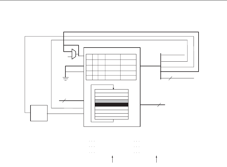
DSP: DESIGNING FOR OPTIMAL RESULTS
68•Xilinx
trick. Figure 4-4 illustrates the control logic and memory layout for this embedded control logic
implementation.
Figure 4-4 demonstrates how the predictable and repeatable control sequence for the coefficient
side of the memory can be embedded into the remaining space of the memory. The coefficient address
value, accumulator Load signal, CE, and WE for the data buffer are precalculated and concatenated on
to the coefficient values. The memory must be used in 512 x 36 mode, instead of 1024 x 18 mode. The
individual signals are split up correctly on the output of the memory. This costs nothing in logic
utilization apart from routing.
Due to the feedback nature of the address line, it is important to set the initial state of the dual-
port block RAM’s output register to effectively “kick- start” the MAC process. The initial values need
to be different from each other to start the correct addressing, however, the silicon forces them to be
the same. This changes the 1-bit masking of the LSB of the coefficient address such that the first value
is ‘0’ instead of the initialized value of ‘1’. The initial value of the output latch is on the address bus the
next cycle and, by unmasking the LSB, the count is successfully kick-started. Because the coefficients
are placed in the upper half of the memory, only a single LSB must be masked, not the complete
address bus. The masking signal can take the form of a reset signal or a registered permanent value to
get the required single cycle mask. Each address concatenated onto its respective coefficient is the next
required address (ahead by two cycles due to the output latch and register) to keep cycling through the
coefficients.
This technique enables a reduction in the control logic required for the MAC FIR filter, but it can
only be exploited when the number of coefficients is smaller than 256 for greater than 9-bit data (256
Figure 4-4: Control Logic Using Embedded Control Technique
en addr
Counter
N -> (2N–1)
DIN A
WE_A
data addr
coef addr
WE
DIN B
DOUT B
DOUT A
RAM must be:
- Read before Write
- Output Register On
Dual-Port RAM
WE_B
CE
coef addr
18
17 ... 026 ... 18272829
coef addr coef (0)
coef (N)
loadCEWE
18
Coefficients
18
.
.
.
.
.
..
.
.
.
..
..
.
.
.
.
.
.
.
.
..
.
.
.
.
.
.
.
.
.
.
.
.
.
.
.
Load ACC
0
coef
addr(0)
DIN D1 X X X
Coeff Addr
Data Addr
XX XD2 X X X X D3 X X X
0 1 2 3 94 95 94 9503212301
96 97 98 99 190 191 191 9796 98 189 190 190 96191 97
WE WE
UG073_c3_05_090204

MAC FIR FILTERS
Xilinx • 69
data and 256 coefficient elements are required to be stored). Table 4-2 highlights the smaller resource
utilization.
Rounding
As noted earlier, the number of bits on the output of the filter is much larger than the number of bits
on the input, and must be reduced to a manageable width. The output can be truncated by simply
selecting the MSBs required from the filter. However, truncation introduces an undesirable DC data
shift due to the nature of two’s complement numbers. Negative numbers become more negative, and
positive numbers also become more negative. The DC shift can be improved with the use of symmetric
rounding, where positive numbers are rounded up and negative numbers are rounded down.
The rounding capability built into the DSP48 slice maintains performance and minimizes the use
of the FPGA fabric. This is implemented in the DSP48 slice using the C input port and the Carry-In
port. The rounding is achieved in the following manner:
• For positive numbers: Binary Data Value +
0.10000… and then truncate
• For negative numbers: Binary Data Value +
0.01111... and then truncate
The actual implementation always adds
0.0111… to the data value using the C input port, as in
the negative case, and then adds the extra carry in required to adjust for positive numbers. Table 4-3
illustrates some examples of symmetric rounding.
In the instance of the MAC FIR filter, the C input is available for continued use because the Z
multiplexer is used for the feedback from the P output. Therefore, for rounding to be performed,
either an extra cycle or another DSP48 slice is required. Typically, an extra cycle is used to save on
DSP48 slices. On the extra cycle, OPMODE is changed for the X and Y multiplexers, setting the X
multiplexer to zero and the Y multiplexer to use the C input to add the user-specified requirements for
a negative rounding scenario.
Table 4-2: Control Logic Using Embedded Block RAMs Resource Utilization
Element Slices
Control Counter
5
Total
5
Table 4-3: Symmetric Rounding Examples
Decimal Value Binary Value Add Round Truncate: Finish Rounded Value
2.4375
0010.0111 0010.1111 0010
2
2.5
0010.1000 0011.0000 0011
3
2.5625
0010.1001 0011.0001 0011
3
-2.4375
1101.1001 1110.0000 1110
-2
-2.5
1101.1000 1101.1111 1101
-3
-2.5625
1101.0111 1101.1110 1101
-3
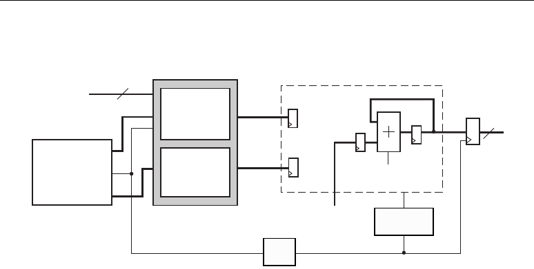
DSP: DESIGNING FOR OPTIMAL RESULTS
70•Xilinx
The Z multiplexer remains unchanged, as the feedback loop is still required, leading to the
opcode being
0101100. The simplified diagram in Figure 4-5 shows how the DSP48 slice functions
during this extra cycle.
Rounding without an Extra Cycle
A trade-off can be made to avoid using the extra cycle required for true symmetric rounding. In this
instance, the rounding constant is added to first inner product when the load of the first inner product
occurs, leading to an OPMODE value of
0110101 instead of 0100101. The carry-in value is applied
on the final cycle to complete the rounding.
The trade-off is using the penultimate accumulated inner product as the basis for rounding,
which is fine unless the penultimate inner product value is very close to zero. In this case, if the value
is positive and the final inner product makes the result negative, leading to a rounding down, an
incorrect result occurs due to the rounding function assuming a positive number instead of a negative.
The last coefficient in typical FIR filters is very small, hence, this case rarely occurs. This form of “not
quite perfect” rounding does save a cycle if absolutely necessary and also gives a significant
improvement over truncation.
Using Distributed RAM for Data and Coefficient Buffers
For smaller-sized MAC FIR filters (typically those under 32 taps), it can be considered wasteful to use
block RAM as a means to store filter input samples and coefficients. Using block RAM for a 16-tap,
18-bit filter, for example, only uses up to 3% of the memory block. Block RAMs are not as abundant
as the smaller distributed RAMs found inside the slice, making them an excellent option for smaller
Figure 4-5: MAC FIR Filter in Rounding Mode
Data Samples
96 x 18
Coefficients
96 x 18
Control
Data Addr
WE
Dual-Port Block RAM
18
18
A
B
CIN
P
Coef Addr
UG073_c3_06_081804
C
Rounding
Constant
OPMODE
Translation
Z
-4
DSP48 Slice
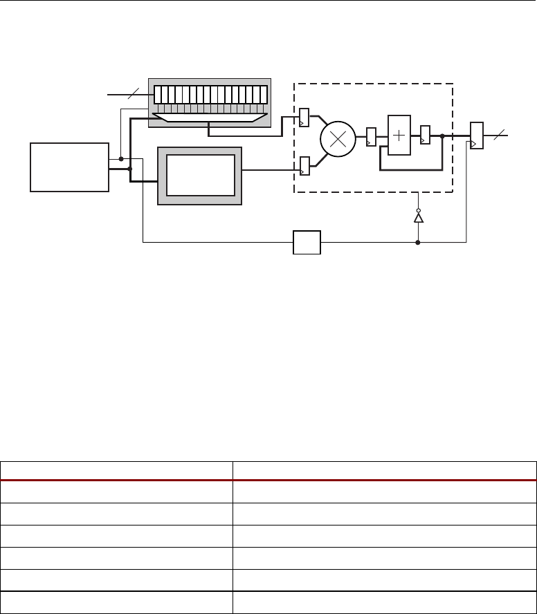
MAC FIR FILTERS
Xilinx • 71
FIR filters. Figure 4-6 illustrates the MAC FIR filter implementation using distributed RAM for the
coefficient bank and an SRL16E for the data buffer.
The resource utilization is still small for these small memories. For a 16-tap (or less), n-bit
memory bank, the cost is n/2 slices. Therefore, for this example, the cost is nine slices per memory
bank (18 slices in total).
The added benefit of using SRL16Es is the embedded shifting capabilities leading to a reduction
in control logic. Only a single count value is required to address both the coefficient buffer and the
data buffer. The terminal count signal is used to write the slower input samples into the data buffer
and capture the results and to load the accumulator with the new set of inner products. The size of the
control logic and memory buffer for a 16-tap, 18-bit data and coefficient FIR is detailed in Table 4-4.
All aspects of the DSP48 and capture register approach to the MAC FIR filter using distributed
RAM are identical to the block RAM based MAC FIR.
Figure 4-6: Tap-Distributed RAM MAC FIR Filter
Table 4-4: Control Logic Resource Utilization
Element Slices
Data Buffer
9
Coefficient Memory
9
Control Counter
2
Relational Operator
1
Capture/Load Delay
1
Total
22
Control
WE
Addr
18
18
A
B
load
P
Coefficients
16 x 18
Single-Port
Distributed Memory
UG073_c3_07_081804
Z
-3
DSP48 Slice
OPMODE = 0100101
SRL16E
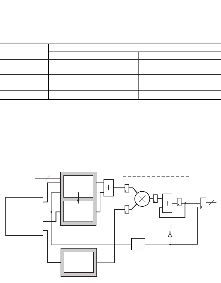
DSP: DESIGNING FOR OPTIMAL RESULTS
72•Xilinx
Performance
Table 4-5 compares the performance of a Virtex-4 MAC FIR filter with a Virtex-II Pro solution.
Overall, the Virtex-4 DSP48 slice greatly reduces the logic fabric resource requirement, improves the
speed of the design, and reduces filter power consumption.
Symmetric MAC FIR Filter
The HDL code provided in the reference design is for a single multiplier MAC FIR filter. other
techniques can also be explored. This section describes how the symmetric nature of FIR filter
coefficients can double the capable sample rate performance of the filter (assuming the same clock
speed). By rearranging the FIR filter equation, the coefficients are exploited as follows:
(X0 x C0) + (Xn x Cn) …
→
(X0 + Xn) x C0 (if C0 = Cn) Equation 4-6
Figure 4-7 shows the architecture for a symmetric MAC FIR filter.
Table 4-5: 18 x 18 MAC FIR Filter (96 Tap) Comparison
Parameter
18 x 18 MAC FIR Filter (96 Tap)
Virtex-II Pro FPGA Virtex-4 FPGA
Size
99 slices, 1 Embedded Multiplier,
1 block RAM
24 slices, 1 DSP48 Slice,
1 block RAM
Performance
(Clock Speed)
3.125 MSPS
250 MHz
4.69 MSPS
450 MHz
Power
170mW 57mW
Figure 4-7: Symmetric MAC FIR Filter
Data Samples
96 x 18
Dual Read
Access
Control
Data1 Addr
WE
Data2 Addr
Dual-Port Block RAM
17
18
A
B
load
P
Coefficients
48 x 18
Single-Port Block RAM
Coef Addr
UG073_c3_08_020405
DSP48 Slice
OPMODE = 010010
Z
-4
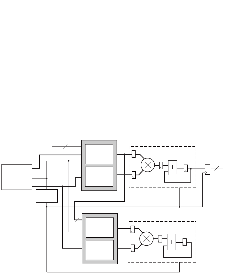
MAC FIR FILTERS
Xilinx • 73
There are limitations to using the symmetric MAC FIR filter. Due to the 1-bit growth from the
pre-adder shown in Figure 4-5, the data input to the filter must be less than 18 bits to fit into one
DSP48 slice. If necessary, the pre-adder can be implemented in slices or in another DSP48 slice.
The performance of this fabric-based adder represents the critical path through the filter and
limits the maximum clock speed. There are extra resources required for the filter to support symmetry.
Three memory ports are needed along with the pre-adder. The control portion increases in resource
utilization since the data is read out of one port in a forward direction and in reverse on the second
port. This technique should only be utilized when extra sample rate performance is required.
Dual-Multiplier MAC FIR Filter
Another technique used to improve the data throughput of an MAC FIR filter is to increase the
number of multipliers used to process the data. This introduces parallelism into the DSP design, and
can be extrapolated into completely parallel techniques supporting the highest of sample rates.
Figure 4-8 and Figure 4-9 illustrate how a dual-multiplier MAC FIR filter can be implemented
using two DSP slices. Figure 4-8 shows the accumulation of the coefficients of each of the two MAC
engines. These partial results must be combined together and then rounded to achieve the final result.
This process uses an extra cycle and the OPMODE switching of the DSP48 slice. This extra cycle is
illustrated in Figure 4-9.
Figure 4-8: Dual-Multiplier MAC FIR Filter
Data Samples
43 x 18
Coefficients
43 x 18
Control
Data Addr
WE
Coef Addr
DSP48 Slice
18
18
A
B
A
B
P
Dual-Port Block RAM
Data Samples
43 x 18
Coefficients
43 x 18
Dual-Port Block RAM
DSP48 Slice
18
OPMODE = 010010
OPMODE
Translation
OPMODE = 010010
UG073_c3_09_081804
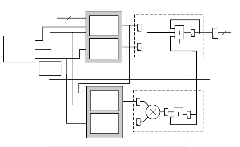
DSP: DESIGNING FOR OPTIMAL RESULTS
74•Xilinx
Conclusion
MAC FIR filters are commonly used in DSP applications. With the introduction of the Virtex-4
DSP48 slice, this function can be achieved in a smaller area, while at the same time producing higher
performance with less power resources. Designers have tremendous flexibility in determining the
desired implementation as well as the ability to change the implementation parameters.
Each specification and design scenario brings a different set of restrictions for the design. Several
more techniques are discussed in the next chapters. The ability to "tune" a filter in an existing system
or to have multiple filter settings is a distinct advantage. The HDL and System Generator for DSP
reference designs are easily modified to achieve specific requirements, such as different coefficients,
smaller data and coefficient bit widths, and coefficient values.
Figure 4-9: Dual-Multiplier MAC FIR Filter with Extra Cycle
Data Samples
43 x 18
Coefficients
43 x 18
Control
Data Addr
WE
Coef Addr
DSP48 Slice
18
18
A
B
A
B
P
Dual-Port Block RAM
Data Samples
43 x 18
Coefficients
43 x 18
Dual-Port Block RAM
DSP48 Slice
18
OPMODE = 0100101
OPMODE
Translation
OPMODE = 0011110
UG073_c3_10_081804
Rounding
Constant
Cin

Xilinx • 75
Chapter 5
Parallel FIR Filters
This chapter describes the implementation of high-performance, parallel, full-precision FIR filters
using the DSP48 slice in a Virtex-4 device. Because the Virtex-4 architecture is flexible, it is practical
to construct custom FIR filters to meet the requirements of a specific application. Creating optimized,
parallel filters saves either resources and potential clock cycles.
This chapter demonstrates two parallel filter architectures: the Transposed and Systolic Parallel
FIR filters. The reference design files in VHDL and Verilog permit filter parameter changes including
coefficients and the number of taps.
Overview
There are many filtering techniques available to signal processing engineers. A common filter
implementation for high-performance applications is the fully parallel FIR filter. Implementing this
structure in the Virtex-II architecture uses the embedded multipliers and slice based arithmetic logic.
The Virtex- 4 DSP48 slice introduces higher performance multiplication and arithmetic capabilities
specifically designed to enhance the use of parallel FIR filters in FPGA-based DSP.
Parallel FIR Filters
A wide variety of filter architectures are available to FPGA designers due to the “liquid hardware”
nature of FPGAs. The type of architecture chosen is typically determined by the amount of processing
required in the available number of clock cycles. The two most important factors are:
• Sample Rate (Fs)
• Number of Coefficients (N)
In Figure 5-1, as the sample rate increases and the number of coefficients increase, the
architecture selected for a desired FIR filter becomes a more parallel structure involving more
multiply and add elements. Chapter 4, “MAC FIR Filters” addresses the details of the sequential
processing FIR filters including the single and dual MAC FIR filter. This chapter investigates the
other extreme of the fully parallel FIR filter as required to filter the fastest data streams.
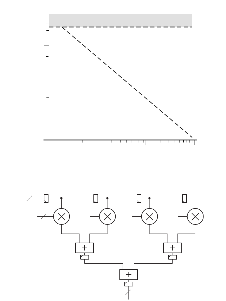
DSP: DESIGNING FOR OPTIMAL RESULTS
76•Xilinx
The basic parallel architecture, shown in Figure 5-2, is referred to as the Direct Form Type 1.
Figure 5-1: Selecting Filter Architectures
Figure 5-2: Direct Form Type 1 FIR Filter
10
50
500
400
300
200
100
1
Semi-Parallel FIR Filters
(Chapter 5)
Sequential FIR Filters (Chapter 3)
Parallel FIR Filters (Chapter 4)
10
20 50 500200
100 1000
UG073_c4_02_082404
Number of Coefficients (N)
Log Scale
Sample Rate (MHz)
Log Scale
5
1
0.5
5
h3
18
38
18
h2 h1 h0
UG073_c4_03_060404
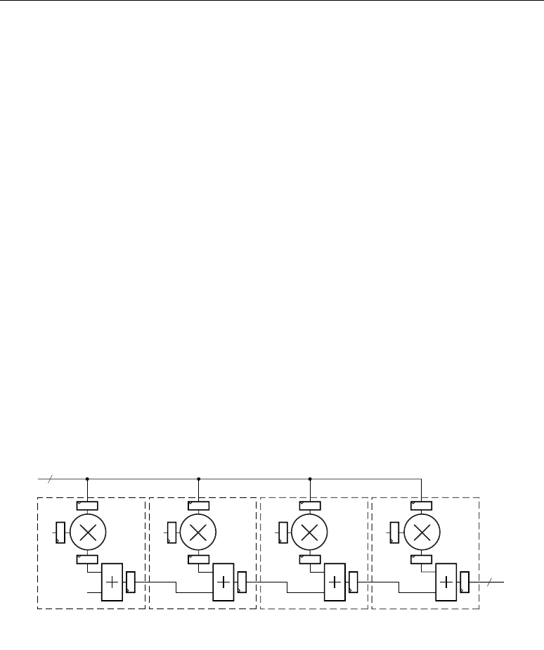
PARALLEL FIR FILTERS
Xilinx • 77
This structure implements the general FIR filter equation of a summation of products as defined
in Equation 5-1.
Equation 5-1
In Equation 5-1, a set of N coefficients is multiplied by N respective data samples. The results are
summed together to form an individual result. The values of the coefficients determine the
characteristics of the filter (e.g., a low-pass filter).
The history of data is stored in the individual registers chained together across the top of the
architecture. Each clock cycle yields a new complete result and all multiplication and arithmetic
required occurs simultaneously. In sequential FIR filter architectures, the data buffer is created using
Virtex-4 dedicated block RAMs or distributed RAMs. This demonstrates a trend; as algorithms
become faster, the memory requirement is reduced. However, the memory bandwidth increases
dramatically since all N coefficients must be processed at the same time.
The performance of the Parallel FIR filter is calculated in Equation 5-2.
Maximum Input Sample Rate = Clock Speed Equation 5-2
The bit growth through the filter is the same for all FIR filters and is explained in the section “Bit
Growth” in Chapter 4.
Transposed FIR Filter
The DSP48 arithmetic units are designed to be easily and efficiently chained together using dedicated
routing between slices. The Direct Form Type I uses an adder tree structure. This makes it difficult to
chain the blocks together. The Transposed FIR filter structure (Figure 5-3) is more optimal for use
with the DSP48 Slice.
The input data is broadcast across all the multipliers simultaneously, and the coefficients are
ordered from right to left with the first coefficient, h0, on the right. These results are fed into the
pipelined adder chain acting as a data buffer to store previously calculated inner products in the adder
chain. The rearranged structure yields identical results to the Direct Form structure, but gains from
the use of an adder chain. This different structure is easily mapped to the DSP48 slice without
Figure 5-3: Transposed FIR Filter
y
n
x
ni–
h
i
i0=
N1–
∑
=
h3
B
18
0
h2
B
h1
B
h0
B
P
DSP48 Slice
OPMODE = 0000101
DSP48 Slice
OPMODE = 0010101
DSP48 Slice
OPMODE = 0010101
DSP48 Slice
OPMODE = 0010101
UG073_c4_04_081104
20
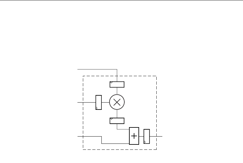
DSP: DESIGNING FOR OPTIMAL RESULTS
78•Xilinx
additional external logic. If more coefficients are required, then more DSP48 slices are required to be
added to the chain.
The configuration of the DSP48 slice for each segment of the Transposed FIR filter is shown in
Figure 5-4. Apart from the very first segment, all processing elements are to be configured as in
Figure 5-4. OPMODE is set to multiply mode with the adder combining the results from the
multiplier and from the previous DSP48 slice through the dedicated cascade input (PCIN). OPMODE
is set to binary
0010101.
Advantages and Disadvantages
The advantages to using the Transposed FIR filter are:
• Low Latency: The maximum latency never exceeds the pipelining time through the slice
containing the first coefficient. Typically, this is three clock cycles between the data input and
the result appearing.
• Efficient Mapping to the DSP48 Slice: Mapping is enabled by the adder chain structure of
the Transposed FIR filter. This extendable structure supports both large and small FIR filters.
• No External Logic: No external FPGA fabric is required, enabling the highest possible
performance to be achieved.
The disadvantage to using the Transposed FIR filter is:
• Limited Performance: Performance may be limited by a high fanout input signal if there are
a large number of taps.
Resource Utilization
An N coefficient filter uses “N” DSP48 slices. A design cannot use symmetry to reduce the number of
DSP48 slices when using the Transposed FIR filter structure.
Figure 5-4: Transpose Multiply-Add Processing Element
UG073_c5_05_081104
DSP48 Slice
OPMODE = 0010101
A
B
PCOUT
PCIN
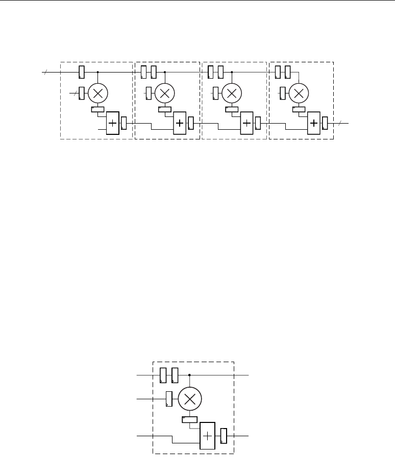
PARALLEL FIR FILTERS
Xilinx • 79
Systolic FIR Filter
The systolic FIR filter is considered an optimal solution for parallel filter architectures. The systolic
FIR filter also uses adder chains to fully utilize the DSP48 slice architecture (Figure 5-5).
The input data is fed into a cascade of registers acting as a data buffer. Each register delivers a
sample to a multiplier where it is multiplied by the respective coefficient. In contrast to the
Transposed FIR filter, the coefficients are aligned from left to right with the first coefficients on the
left side of the structure. The adder chain stores the gradually combined inner products to form the
final result. As with the Transposed FIR filter, no external logic is required to support the filter and
the structure is extendable to support any number of coefficients.
The configuration of the DSP48 slice for each segment of the Systolic FIR filter is shown in
Figure 5-6. Apart from the very first segment, all processing elements are to be configured as shown
in Figure 5-6. OPMODE is set to multiply mode with the adder combining the results from the
multiplier and from the previous DSP48 slice through the dedicated cascade input (PCIN). OPMODE
is set to binary
0010101. The dedicated cascade input (BCIN) and dedicated cascade output
(BCOUT) are used to create the necessary input data buffer cascade.
Figure 5-5: Systolic FIR Filter
Figure 5-6: Systolic Multiply-Add Processing Element
h0
B
18
0
h1 h2 h3
P
DSP48 Slice
OPMODE = 0000101
DSP48 Slice
OPMODE = 0010101
DSP48 Slice
OPMODE = 0010101
DSP48 Slice
OPMODE = 0010101
UG073_c6_06_081104
18
20
ug073_c4_07_081104
DSP48 Slice
OPMODE = 0010101
A
PCOUTPCIN
BCOUTBCIN
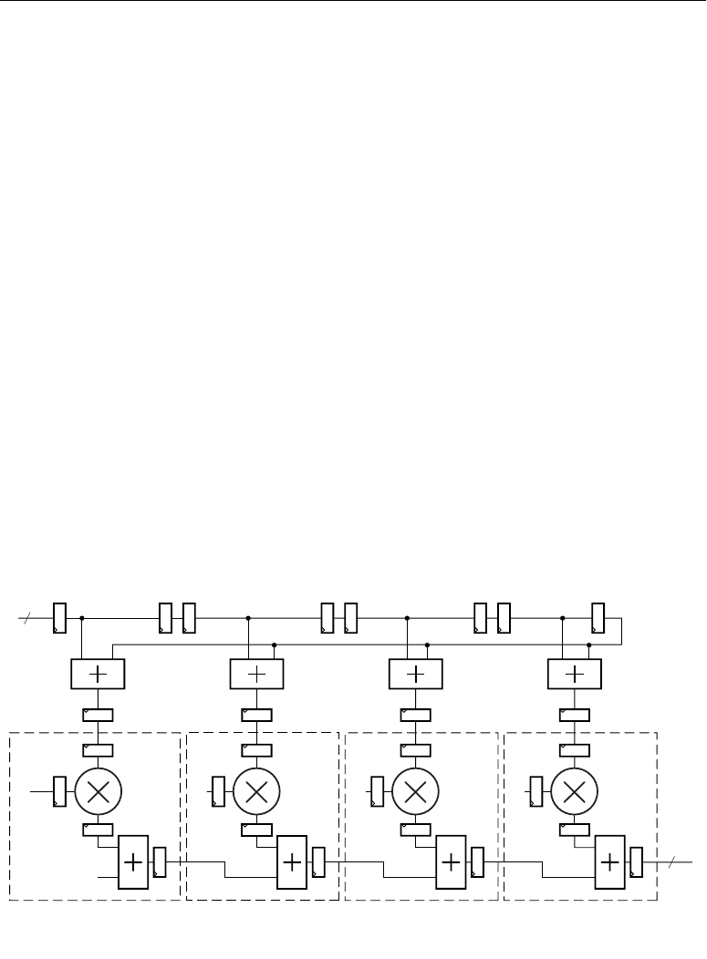
DSP: DESIGNING FOR OPTIMAL RESULTS
80•Xilinx
Advantages and Disadvantages
The advantages to using the Systolic FIR filter are:
• Highest Performance: Maximum performance can be achieved with this structure because
there is no high fanout input signal. Larger filters can be routing-limited if the number of
coefficients exceeds the number of DSP slices in a column on a device.
• Efficient Mapping to the DSP48 Slice: Mapping is enabled by the adder chain structure of
the Systolic FIR Filter. This extendable structure supports large and small FIR filters.
• No External Logic: No external FPGA fabric is required, enabling the highest possible
performance.
The disadvantage to using the Systolic FIR filter is:
• Higher Latency: The latency of the filter is a function of how many coefficients are in the
filter. The larger the filter, the higher the latency.
Resource Utilization
An N coefficient filter uses “N” DSP48 slices.
Symmetric Systolic FIR Filter
In Chapter 4, “MAC FIR Filters,” symmetry was examined and an implementation was illustrated to
exploit this symmetric nature of the coefficients. Exploiting symmetry is extremely powerful in
Parallel FIR filters because it halves the required number of multipliers, which is advantageous due to
the finite number of DSP48 slices. Equation 5-3 demonstrates how the data is pre-added before being
multiplied by the single coefficient.
(X0 x C0) + (Xn x Cn) … ⎝ (X0 + Xn) x C0 (if C0 = Cn) Equation 5-3
Figure 5-7 shows the implementation of this type of Systolic FIR Filter structure.
Figure 5-7: Symmetric Systolic FIR
h0
BBBB
17
0
h1 h2 h3
P
DSP48 Slice
OPMODE = 0000101
DSP48 Slice
OPMODE = 0010101
DSP48 Slice
OPMODE = 0010101
DSP48 Slice
OPMODE = 0010101
UG073_c6_10_082404
38
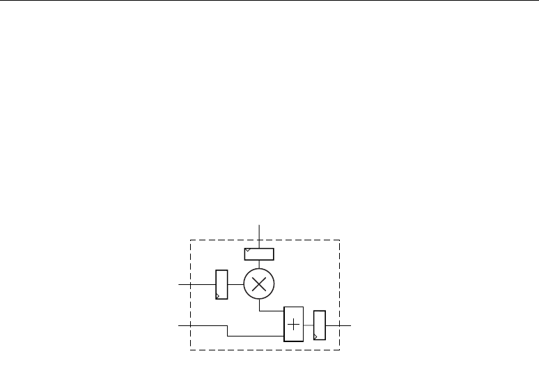
PARALLEL FIR FILTERS
Xilinx • 81
In this structure, DSP48 slices have been traded off for Fabric slices. From a performance
viewpoint, to achieve the full speed of the DSP48 slice, the fabric 18-bit adder has to run at the same
speed. To achieve this, register duplication can be performed on the output from the last tap that feeds
all the other multipliers.
The two register delay in the input buffer time series is implemented as an SRL16E and a register
output to save on logic area. A further benefit of the symmetric implementation is the reduction in
latency, due to the adder chain being half the length.
Figure 5-8 shows the configuration of the DSP48 slice for each segment of the Symmetric Systolic
FIR filter. Apart from the very first segment, all processing elements are to be configured as in
Figure 5-8. OPMODE is set to multiply mode with the adder combining results from the multiplier
and from the previous DSP48 slice via the dedicated cascade input (PCIN). OPMODE is set to binary
0010101.
Resource Utilization
An N symmetric coefficient filter uses N DSP48 slices. The slice count for the pre-adder and input
buffer time series is a factor of the input bit width (n) and N. The equation for the size in slices is:
((n+1) * (N/2)) + (n/2) Equation 5-4
For the example illustrated in Figure 5-7, the size is (17+1) * 8/2 + 17/2 = 81 slices.
Rounding
The number of bits on the output of the filter is much larger than the input and must be reduced to a
manageable width. The output can be truncated by simply selecting the MSBs required from the filter.
However, truncation introduces an undesirable DC data shift. Due to the nature of two's complement
numbers, negative numbers become more negative and positive numbers also become more negative.
The DC shift can be improved with the use of symmetric rounding, where positive numbers are
rounded up and negative numbers are rounded down.
The rounding capability in the DSP48 slice maintains performance and minimizes the use of the
FPGA fabric. This is implemented in the DSP48 slice using the C input port and the Carry In port.
Rounding is achieved by:
For positive numbers: Binary Data Value +
0.10000… and then truncate
For negative numbers: Binary Data Value +
0.01111... and then truncate
Figure 5-8: Symmetric Systolic Multiply-Add (MADD) Processing Element
UG073_c5_11_082404
DSP48 Slice
OPMODE = 0010101
A
B
PCOUT
PCIN
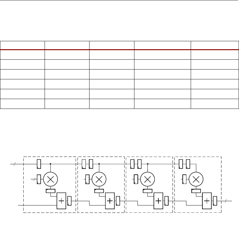
DSP: DESIGNING FOR OPTIMAL RESULTS
82•Xilinx
The actual implementation always adds
0.0111… to the data value through the C port input as
in the negative case, and then adds the extra carry in required to adjust for positive numbers. Table 5-1
illustrates some examples of symmetric rounding.
For both the Transposed and Systolic Parallel FIR filters, the C input is used at the beginning of
the adder chain to drive the carry value into the accumulated result. The final segment uses the MSB
of the PCIN as the carry-in value to determine if the accumulated product is positive or negative.
CARRYINSEL is used to select the appropriate carry-in value. If positive, the carry-in value is used,
and if negative, the result is kept the same (see Figure 5-9).
The one problem with this solution occurs when the final accumulated inner product input to the
final DSP48 slice is very close to zero. If the value is positive and the final inner product makes the
result negative (leading to a rounding down), then an incorrect result occurs because the rounding
function assumes a positive number instead of a negative. The last coefficient in typical FIR filters is
very small, so this situation rarely occurs. However, if absolute certainty is required, an extra DSP48
Table 5-1: Symmetric Rounding Examples
Decimal Value Binary Value Add Round Truncate: Finish Rounded Value
2.4375
0010.0111 0010.1111 0010
2
2.5
0010.1000 0011.0000 0011
3
2.5625
0010.1001 0011.0001 0011
3
–2.4375
1101.1001 1110.0000 1110
–2
–2.5
1101.1000 1101.1111 1101
–3
–2.5625
1101.0111 1101.1110 1101
–3
Figure 5-9: Systolic FIR Filter with Rounding
h0
B
18
0.49999
C
h1 h2 h3
P
DSP48 Slice
OPMODE = 0'b0000101
DSP48 Slice
OPMODE = 0'b0010101
DSP48 Slice
OPMODE = 0'b0010101
DSP48 Slice
OPMODE = 0'b0010101
Carryinsel = 01
UG073_c4_08_060704
18
18
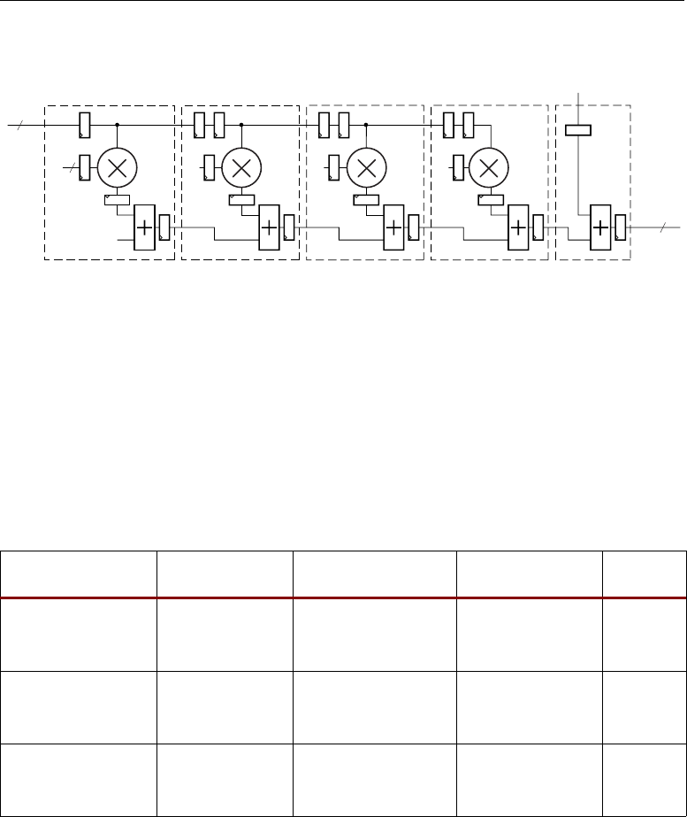
PARALLEL FIR FILTERS
Xilinx • 83
slice can perform the rounding function (see Figure 5-10). A Transposed FIR filter can have exactly the
same problem as the Systolic FIR filter.
Performance
When examining the performance of a Virtex-4 Parallel FIR filter, a Virtex-II Pro design is a valuable
reference. Table 5-2 illustrates the ability of the Virtex-4 DSP48 slice to greatly reduce logic fabric
resources requirements while improving the speed of the design and reducing the power utilization of
the filter.
Figure 5-10: Systolic FIR Filter with Separate Rounding Function
Table 5-2: Performance Analysis
Filter Type Device Family Size Performance
Power
(Watts)
18 x 18 Parallel
Transposed FIR Filter
(51 Tap Symmetric)
Virtex-II Pro
FPGA
1860 Slices
26 Embedded
Multipliers
300 MHz Clock
Speed
300 MSPS
TBD
18 x 18 Parallel
Systolic FIR Filter
(51 Tap Symmetric)
Virtex-II Pro
FPGA
2958 Slices
26 Embedded
Multipliers
300 MHz Clock
Speed
300 MSPS
TBD
18 x 18 Parallel
Transposed FIR Filter
(51 Tap Symmetric)
Virtex-4 FPGA 0 Slices
51 DSP48 Slices
400 MHz Clock
Speed
400 MSPS
TBD
h0
B
18
0
C
h1
h2 h3
C
0.4999
P
DSP48 Slice
OPMODE = 0'b0000101
DSP48 Slice
OPMODE = 0'b0010101
DSP48 Slice
OPMODE = 0'b0010101
DSP48 Slice
OPMODE = 0'b0010101
DSP48 Slice
OPMODE = 0'b0011101
Carryinsel = 01
UG073_c4_09_061304
18
18

DSP: DESIGNING FOR OPTIMAL RESULTS
84•Xilinx
Conclusion
Parallel FIR filters are commonly used in high-performance DSP applications. With the introduction
of the Virtex-4 DSP48 slice, DSPs can be achieved in a smaller area, thereby producing higher
performance with less power penalty.
Designers have tremendous flexibility in determining the desired implementation, and also have
the ability to change the implementation parameters. The ability to “tune” a filter in an existing
system or to have multiple filter settings is a distinct advantage. By making the necessary coefficient
changes in the synthesizable HDL code, the reconfigurable nature of the FPGA is fully exploited. The
coefficients can be either hardwired to the A input of the DSP48 slices or stored in small memories and
selected to change the filter characteristics. The HDL and System Generator for DSP reference designs
are easily modified to achieve specific requirements.
17 x 18 Systolic FIR
Filter
(51 Tap Non-
symmetric)
Virtex-4 FPGA 0 Slices
51 DSP48 Slices
450 MHz Clock
Speed
450 MSPS
TBD
17 x 18 Systolic FIR
Filter
(51 Tap Symmetric)
Virtex-4 FPGA 477 Slices
26 DSP48 Slices
400 MHz Clock
Speed
400 MSPS
TBD
Table 5-2: Performance Analysis (Continued)
Filter Type Device Family Size Performance
Power
(Watts)

Xilinx • 85
Chapter 6
Semi-Parallel FIR Filters
This chapter describes the implementation of semi-parallel or hardware-folded, full-precision FIR
filters using the Virtex™-4 DSP48 slice. Because the Virtex-4 architecture is flexible, constructing
FIR filters for specific application requirements is practical. Creating optimum filter structures of a
semi-parallel nature saves resources and potential clock cycles. Therefore, optimum filter structures of
a semi-parallel nature can be created without draining resources or clock cycles.
This chapter demonstrates two semi-parallel filter architectures: the four- multiplier FIR filter
using distributed RAM and the three-multiplier FIR filter using block RAM. These filters illustrate
how resources are saved by using available clock cycles and hardware-folding techniques. Reference
design files are available for system generator in DSP, VHDL, and Verilog. The reference designs
permit filter parameter changes including coefficients and the number of taps.
Overview
A large array of filtering techniques are available to signal processing engineers. A common filter
implementation to exploit available clock cycles, while still achieving moderate to high sample rates,
is the semi-parallel (also known as folded-hardware) FIR filter. In the past, this structure used the
Virtex-II embedded multipliers and slice-based arithmetic logic. However, the Virtex-4 DSP48 slice
introduces higher performance multiplication and arithmetic capabilities to enhance the use of semi-
parallel FIR filters in FPGA-based DSP designs.
Semi-Parallel FIR Filter Structure
A wide variety of filter architectures are available to FPGA designers due to the liquid hardware nature
of FPGAs. The type of architecture is typically determined by the amount of processing required in
the number of available clock cycles. The two most important factors are:
• Sample Rate (Fs)
• Number of Coefficients (N)
As illustrated in Figure 6-1, as the sample rate increases and the number of coefficients increase,
the architecture selected for a desired FIR filter becomes a more parallel structure involving more
multiply-add elements. Chapter 4, “MAC FIR Filters” addresses the details of sequential processing
FIR filters including the single and dual MAC FIR Filter. Chapter 5, “Parallel FIR Filters”
investigates the polar extreme of the fully-parallel FIR filter required for the highest sample rate
filters. This chapter examines the common scenario requiring multiple processing elements working
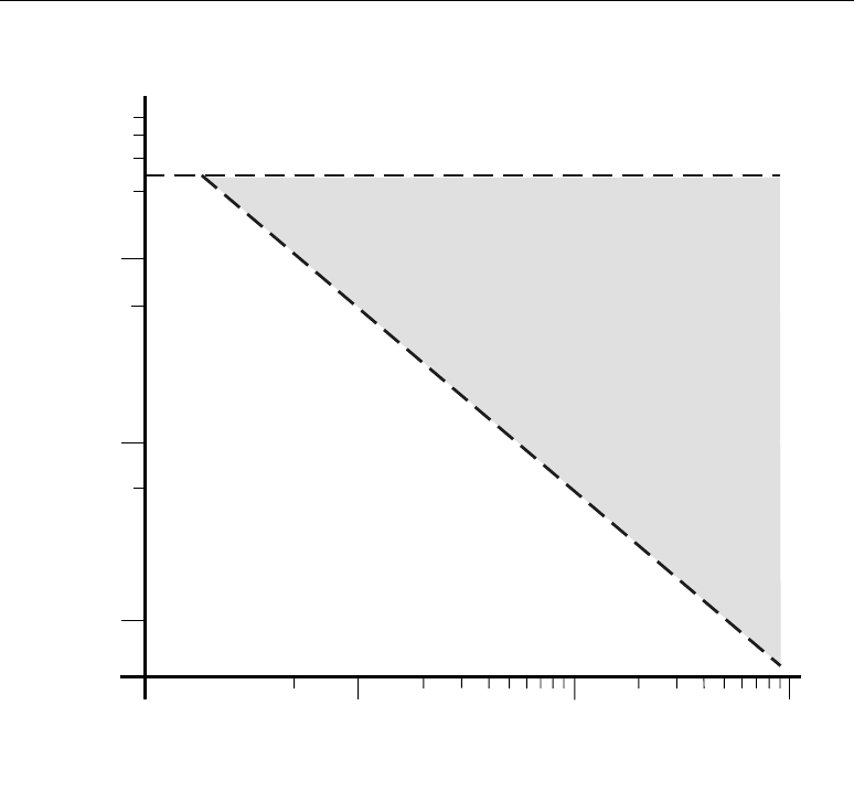
DSP: DESIGNING FOR OPTIMAL RESULTS
86•Xilinx
over numerous clock cycles to achieve the result. These techniques are often referred to as semi-parallel
and are used to maximize efficiency of the filter (see Figure 6-1).
The semi-parallel FIR structure implements the general FIR filter equation of a summation of
products defined as shown in Equation 6-1.
Equation 6-1
Here a set of N coefficients is multiplied by N respective time series data samples, and the results
are summed together to form an individual result. The values of the coefficients determine the
characteristics of the filter (for example, a low-pass filter).
Along with achievable clock speed and the number of coefficients (N), the number of multipliers
(M) is also a factor in calculating semi-parallel FIR filter performance. The following equation
demonstrates how the more multipliers used, the greater the achievable performance of the filter.
Figure 6-1: Selecting Filter Architectures
10
50
500
400
300
200
100
1
Semi-Parallel FIR Filters
(Chapter 5)
Sequential FIR Filters (Chapter 3)
Parallel FIR Filters (Chapter 4)
10
20 50 500200
100 1000
UG073_c5_01_082404
Number of Coefficients (N)
Log Scale
Sample Rate (MHz)
Log Scale
5
1
0.5
5
y
n
x
ni–
h
i
i0=
N1–
∑
=
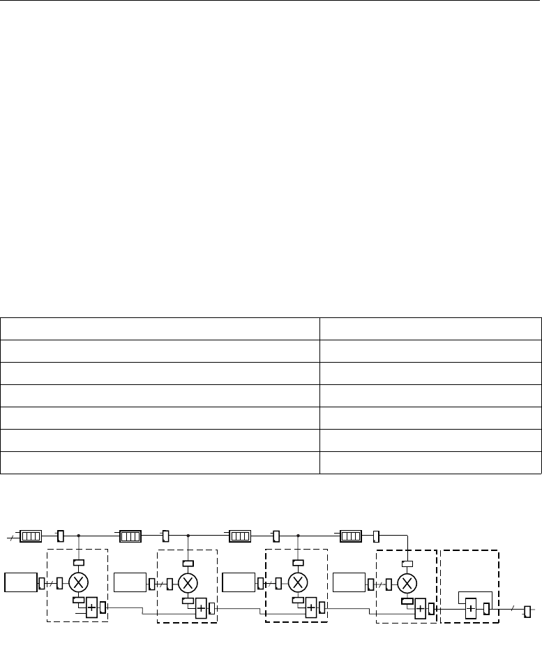
SEMI-PARALLEL FIR FILTERS
Xilinx • 87
Maximum Input Sample rate = (Clock speed / Number of Coefficients) x Number of Multipliers
The above equation is rearranged to determine how many multipliers to use for a particular semi-
parallel architecture:
Number of Multipliers = (Maximum Input Sample rate x Number of Coefficients) / Clock speed
The number of clock cycles between each result of the FIR filter is determined by the following
equation:
Number of Clock cycles per result = Number of Coefficients / Number of Multipliers
The bit growth on the output of the filter is the same as for all FIR filters and is explained in “Bit
Growth” in Chapter 4. The large 48-bit internal precision of the DSP48 slice means that little concern
needs to be paid to the internal bit growth of the filter.
Four-Multiplier, Distributed-RAM-Based, Semi-Parallel FIR Filter
Once the required number of multipliers is determined, there is an extendable architecture using the
DSP48 slice for use as the basis of the filter. This section assumes the specifications in Table 6-1
describe the filter implementation and its functions.
Figure 6-2 illustrates the main structure for the four-multiplier, semi-parallel FIR filter.
The DSP48 slice arithmetic units are designed to be chained together easily and efficiently due to
dedicated routing between slices. Figure 6-2 shows how the four DSP48 slice multiply-add elements
are cascaded together to form the main part of the filter structure. Figure 6-3 provides a detailed view
Table 6-1: Four-Multiplier, Semi-Parallel FIR Filter Specifications
Sampling Rate
112.5 MSPS
Number of Coefficients
16
Assumed Clock Speed
450 MHz
Input Data Width
18 Bits
Output Data Width
18 Bits
Number of Multipliers
4
Number of Clock Cycles Between Each Result
4
Figure 6-2: Four-Multiplier, Semi-Parallel FIR Filter in Accumulation Mode
UG073_c5_02_081104
DSP48 Slice
OPMODE = 0110101
18
Coefficients
4 x 18
Coefficients
4 x 18
Coefficients
4 x 18
Coefficients
4 x 18
0
B
DSP48 Slice
OPMODE = 0010101
18
B
DSP48 Slice
OPMODE = 0010101
18
B
DSP48 Slice
OPMODE = 0010101
18
B
DSP48 Slice
OPMODE = 0010010
SRL16E SRL16E SRL16E SRL16E
18
CE
CE
CE1
CE1
CE2
CE2 CE3
40
CE4
P
PCIN
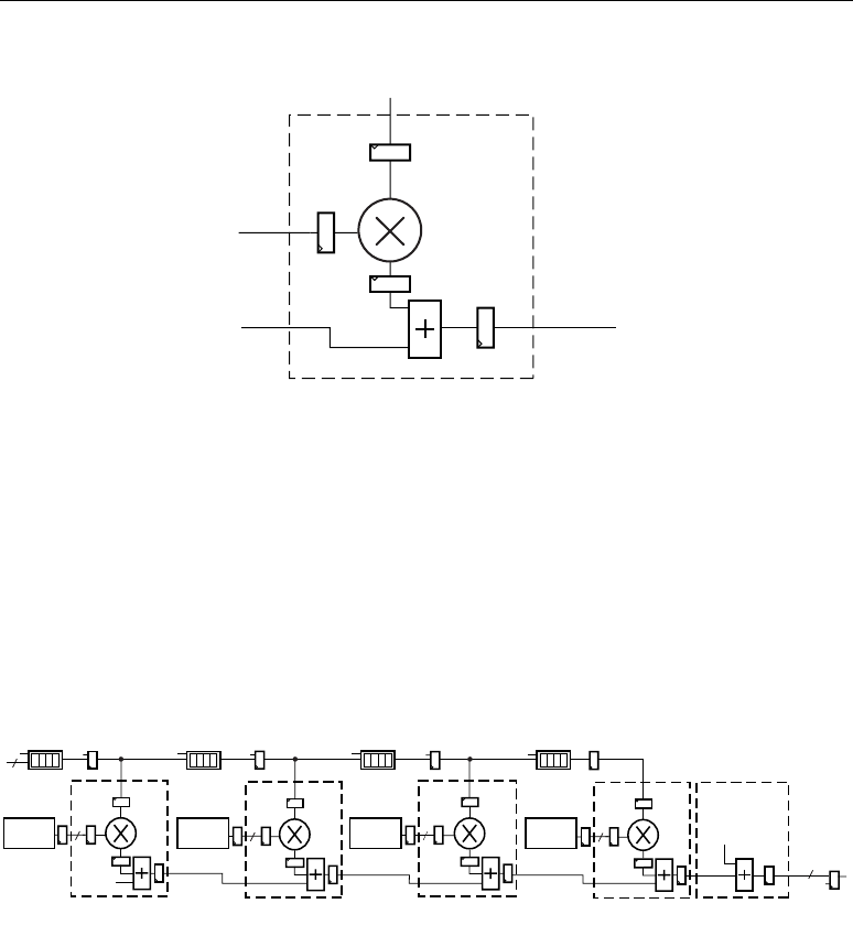
DSP: DESIGNING FOR OPTIMAL RESULTS
88•Xilinx
of the main multiply-add elements. The two pipeline registers are used on the B input to compensate
for the register on the output of the coefficient memory.
An extra DSP48 slice is required on the end to perform the accumulation of the partial results,
thus creating the final result. A new result is created every four cycles. Every four cycles, the
accumulation must be reset to the first partial value of the next result. As in the MAC FIR Filter, this
reset (or load) is achieved by changing the OPMODE value of the DSP48 slice for a single cycle.
OPMODE is changed from binary
0010010 to binary 0010000 (just a single bit change). At the
same time, the capture register is also enabled, and the final result is stored on the output (see
Figure 6-4).
Control logic is required to make this dynamic change occur. The specifics are detailed in
“Control Logic and Address Sequencing,” page 90.
Data Memory Buffers
This example uses eight memories. Four SRL16Es are used as data buffers. Each SRL16E holds the
four samples needed for the result. They are written to once every four cycles (the input data rate is 4x
slower than the internal rate), and the shifting characteristic of the SRL16E is exploited to pass old
Figure 6-3: Detailed Diagram of a Single Multiply-Add Element
Figure 6-4: Four-Multiplier, Semi-Parallel FIR Filter at the Start of a New Result Cycle
UG073_c5_03_081104
DSP48 Slice
OPMODE = 0010101
A
B
PCIN PCOUT
UG073_c5_02_081104
DSP48 Slice
OPMODE = 0110101
18
Coefficients
4 x 18
Coefficients
4 x 18
Coefficients
4 x 18
Coefficients
4 x 18
0
B
DSP48 Slice
OPMODE = 0010101
18
B
DSP48 Slice
OPMODE = 0010101
18
B
DSP48 Slice
OPMODE = 0010101
18
B
DSP48 Slice
OPMODE = 0010000
SRL16E SRL16E SRL16E SRL16E
18
CE
CE
CE1
CE1
CE2
CE2 CE3
40
0
CE4
P
PCIN
SEMI-PARALLEL FIR FILTERS
Xilinx • 89
samples along the time series buffer. The extra register on the output of each data buffer is required to
match up the data buffer pipeline with the extra delay caused by the adder chain. The extra register
should not cost extra resources, because it is already present in the slice containing the SRL16E (see
Figure 6-5).
As long as the depth does not exceed 16, the resources required for each of these input memory
buffers is determined by the bit width of the input data (n). Therefore, n/2 SliceM is required for each
memory buffer, leading to nine slices per buffer in this filter example. For depths up to 32, resources
are a little more than doubled because two SRL16Es are needed, as well as an extra output multiplexer.
For more information on SliceM, refer to the CLB section in the Virtex-4 User Guide.
Coefficient Memory
The coefficients are divided up into four groups of four. This arrangement is determined by dividing
the total number of coefficients by the number of multipliers used in the implementation. In this
example, if the total number of coefficients is 16, and the number of multipliers is four, four
coefficients per memory are needed.
Note that filters with a total number of coefficients that are integer-divisible by the required
number of multipliers are very desirable. System designers should take this into account when
designing their filters to get the optimal filter specification for the implementation used. Otherwise,
the coefficients will have to be padded with zeros to achieve a number of coefficients that are integer-
divisible by the number of multipliers.
The coefficients are simply split into groups according to their order. The first four in the first
memory, the second four in the second memory, and so on (see Figure 6-6).
Figure 6-5: Single Bit of One Input Memory Buffer
UG073_c5_05_081904
1/2 SliceM
Register
SRL16E
DOUT
ADDR[3:0]
CE
CE CE
DIN

DSP: DESIGNING FOR OPTIMAL RESULTS
90•Xilinx
The adder chain architecture of the DSP48 slice means that each Multiply-Add cascade
multiplication must be delayed by a single cycle so that the results synchronize appropriately when
added together. This delay is achieved by addressing of the memories and is explained in “Control
Logic and Address Sequencing”.
Distributed RAM (refer to Chapter 2, “XtremeDSP Design Considerations,” for detailed
information on distributed RAMs) are used for the coefficient memories. The reason for their use is
that it would be an extremely inefficient usage of the larger block RAMs, especially given their
scarcity versus the smaller abundant distributed RAMs. The larger block RAM comes into play when
the number of coefficients per memory starts to increase to the point where the cost in slice resources
becomes significant (for example, greater than 64).
The total cost of the current example is 36 slices. The coefficient width is 18 bits, and distributed
RAMs cost n/2 slices (that is, nine slices per memory and four memories). For larger distributed RAMs
(larger than 16 elements), the size begins to increase as Write Enable (WE) control logic and an output
multiplexer is needed. The distributed memory v7.0 in the CORE Generator system can be easily used
to create these little distributed RAMs and get accurate size estimates.
Control Logic and Address Sequencing
The Control Logic and Address Sequencing is the most important and complicated aspect of semi-
parallel FIR filters, and getting it right is crucial to the operation of the filter. The control logic is
discussed in two separate sections:
• Memory Addressing
• Clock Enable Sequencing
Memory addressing must provide the necessary delay for each multiply-add element mentioned
in “Coefficient Memory,” page 89, caused by the adder chain. This is not the case when using an adder
tree; the DSP48 slice is most efficiently used in adder chains.
Figure 6-7 illustrates the control logic required to create the necessary memory addressing. The
counter creates the fundamental zero through three count. This is then delayed by one cycle by the use
of a register in the control path. Each successive delay is used to address both the coefficient memory
and the data buffer of their respective multiply-add elements. A single delay for the second multiply-
add element, two delays for the third multiply-add element, etc. Note that this is extensible control
logic for M number of multipliers.
Figure 6-6: Coefficient Memory Arrangement
UG073_c5_06_060804
Coefficients Driving
First DSP48 Slice
Coefficients Driving
Second DSP48 Slice
Coefficients Driving
Third DSP48 Slice
Coefficients Driving
Fourth DSP48 Slice
h0
h1
h2
h3
h4
h5
h6
h7
h8
h9
h10
h11
h12
h13
h14
h15
SEMI-PARALLEL FIR FILTERS
Xilinx • 91
Figure 6-7 also shows clock enable sequencing. A relational operator is required to determine
when the count limited counter resets its count. This signal is High for one clock cycle every four
cycles, to represent the input and output data rates. The Clock Enable signal is delayed by a single
register just like the coefficient address, and each delayed version of the signal is tied to the respective
section of the filter. Refer to Figure 6-2 to see the signal connections to the element. Figure 6-8
illustrates the control logic waveforms changing over time.
Figure 6-7: Control Logic for the Four-Multiplier, Semi-Parallel FIR Filter
Figure 6-8: Control Waveforms for Semi-Parallel FIR Filters
UG073_c5_07_081104
addr
Coefficient
Memory 0
&
Data Buffer 0
Address
Coefficient
Memory 1
&
Data Buffer 1
Address
Coefficient
Memory 2
&
Data Buffer 2
Address
Coefficient
Memory 3
&
Data Buffer 3
Address
Counter
0 -> N/M - 1
N/M - 1
CE CE1 CE2 CE3 CE4
Clock
x(n) x(n-1) x(n-2) x(n-3) x(n-4) x(n-5)
Input Data
y(n-1)0 y(n) y(n-2)
Output Data
00123333322221001 101
Address for First DSP48
Slice MADD Element
Control CE
0213 30123012301230123
Address for Second DSP48
Slice MADD Element
Control CE1
3210 23012 2301 130 230123
Address for Third DSP48
Slice Design Element
Control CE2
2103 12301 1230 023 123012
Address for Fourth DSP48
Slice Design Element
Control CE3
UG073_c5_08_082504
DSP: DESIGNING FOR OPTIMAL RESULTS
92•Xilinx
Resource Utilization
Table 6-2 shows the resources used by a 16-tap, four-multiplier, distributed-RAM-based, semi-
parallel FIR filter.
Three-Multiplier, Block RAM-Based, Semi-Parallel FIR Filter
This section investigates a different filter structure, the three-multiplier, block RAM-based, semi-
parallel FIR filter (see Figure 6-9).
The decision to use this implementation is based on the filter specification. The filter
specifications are described in Table 6-3.
Table 6-2: Resource Utilization
Elements Slices DSP48 Slices
Multiply-Add
5
Input Data Buffers
36
Coefficient Memories
36
Capture Register
20
Main Control Counter
2
Relational Operator
1
Multiply-Add Element Control
9 (3 per extra element)
Total
104 5
Figure 6-9: Three-Multiplier, Block-RAM-Based, Semi-Parallel FIR Filter
Table 6-3: Three-Multiplier, Block RAM-Based, Semi-Parallel FIR Filter Specifications
Parameter Value
Sampling Rate
4.5 MSPS
Number of Coefficients
300
Assumed Clock Speed
450 MHz
Input Data Width
18 Bits
Output Data Width
18 Bits
UG073_c5_09_081104
DSP48 Slice
OPMODE = 0110101
18
0
B
18
Cyclic Data
Buffer
100 x 18
Coefficients
100 x 18
Cyclic Data
Buffer
100 x 18
Coefficients
100 x 18
Cyclic Data
Buffer
100 x 18
Coefficients
100 x 18
DSP48 Slice
OPMODE = 0010101
18
B
DSP48 Slice
OPMODE = 0010101
18
B
DSP48 Slice
OPMODE = 0010010
40
P
CE4
PCIN
WE WE1 WE2

SEMI-PARALLEL FIR FILTERS
Xilinx • 93
The structure is similar to the four-multiplier filter studied earlier. In this instance, the lower
sample rate of the filter specification and the larger number of taps indicates that only three multipliers
are required, each servicing 100 coefficients, leading to a new result yielded every 100 clock cycles.
Each memory buffer is required to hold 100 coefficients and also 100 input data history values.
The dedicated Virtex-4 block RAM can be used in dual-port mode with a cyclic data buffer established
in the first half of the memory to serve the shifting input data series.
Chapter 4, “MAC FIR Filters,” describes using these memories to store the input data series, the
coefficients, and also the control logic required to make the cyclic RAM buffer operate. The rest of the
control logic and data flow is identical to the first filter investigated except that only three multipliers
are serviced, therefore, the control logic can be scaled back by one element. Also note that the WE
signals are the inversion of their respective CE pair.
Table 6-4 shows the resource utilization for the 300-tap, three-multiplier, semi-parallel FIR
filter.
Other Semi-Parallel FIR Filter Structures
As with many DSP functions there are many different ways to implement a function. There is never
one solution fitting all requirements for all specifications. For example, should distributed or block
RAM be used for data storage? Should a systolic or a transposed implementation be used for a given
filter? This chapter describes in detail the different techniques using single-rate FIR filters to get the
maximum performance and low resource utilization using the Virtex-4 architecture.
This section introduces other possible semi-parallel FIR filter implementations and discusses the
advantages and disadvantages of their structures.
Number of Mulipliers
3
Number of Clock Cycles Between Each Result
100
Table 6-4: Resource Utilization
Elements Slices DSP48 Slices Block RAMs
Multiply-Add
4
Input Data Buffers and Coefficient
Memories
3
Capture Register
20
Main Control Counter
5
Relational Operator
1
Multiply-Add Element Control
12 (6 per extra
element)
Total
38 4 3
Table 6-3: Three-Multiplier, Block RAM-Based, Semi-Parallel FIR Filter Specifications
Parameter Value
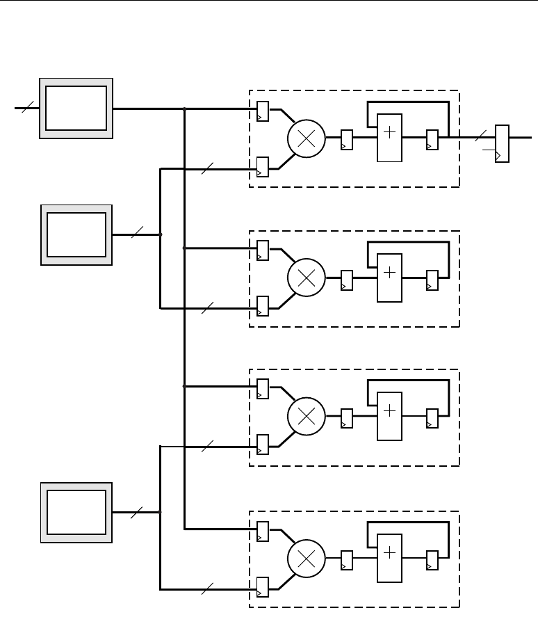
DSP: DESIGNING FOR OPTIMAL RESULTS
94•Xilinx
Semi-Parallel, Transposed, Four-Multiplier FIR Filter
This structure is very different in nature to the main architecture discussed in this chapter (see
Figure 6-10).
Only one data storage buffer is required, typically a block RAM. The data buffer output is also
broadcast to all DSP48 slices. Each DSP48 slice works in accumulator mode until the last cycle of the
calculation, when OPMODE changes to form an adder chain, and then passes the results to the next
DSP48 slice. Actually, four results are being calculated at one time, and the completed result is output
Figure 6-10: Semi-Parallel, Transposed FIR Filter
18
UG073_c5_10_061404
Coefficients
100 x 36
Cyclic Data
Buffer
400 x 18
18
A
B
DSP48 Slice
OPMODE = 0100101
43
CE
18
A
B
DSP48 Slice
OPMODE = 0100101
18
A
B
DSP48 Slice
OPMODE = 0100101
18
A
B
DSP48 Slice
OPMODE = 0100101
Coefficients
100 x 36
36
36
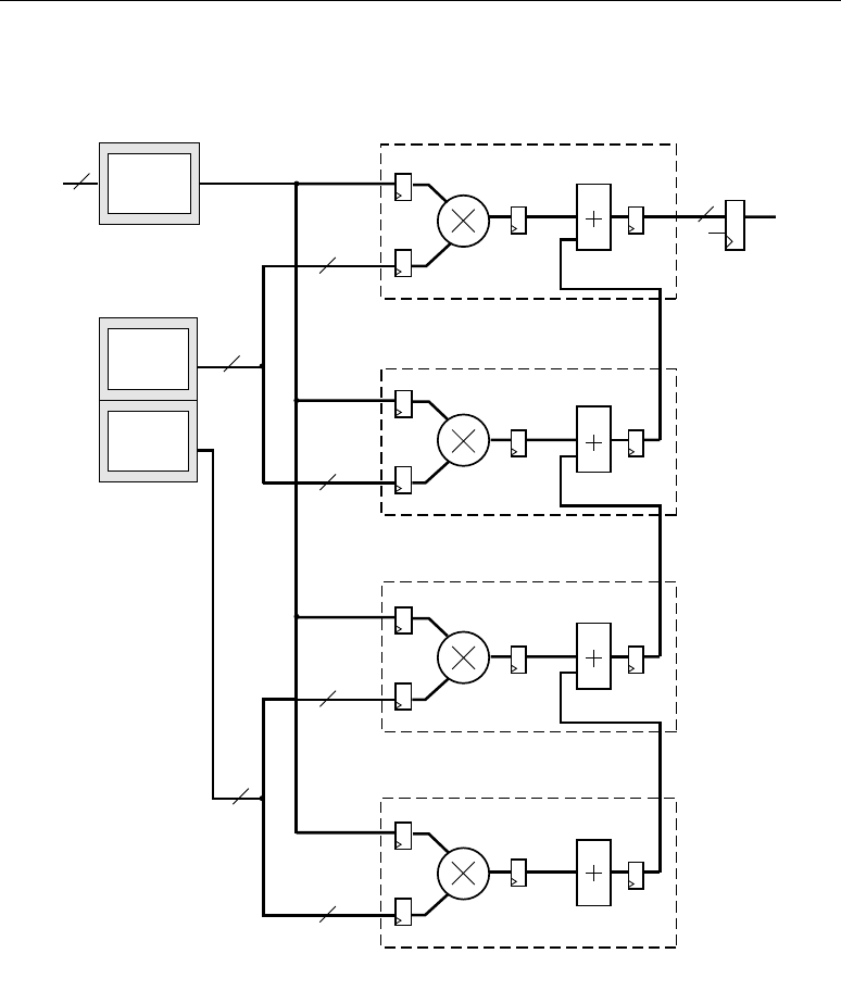
SEMI-PARALLEL FIR FILTERS
Xilinx • 95
from the last DSP48 slice. The previous elements are working on their respective parts of the next
results.
Figure 6-11 shows the filter structure every time the DSP48 slice OPMODE is changed, which
occurs once every result cycle.
Advantages and Disadvantages
The advantages to using the Semi-Parallel, Transposed FIR filter are:
• Lower resource utilization due to one less DSP48 slice required and a single input memory
buffer.
Figure 6-11: Semi-Parallel, Transposed FIR Filter (Combination of the Results)
18
UG073_c5_11_060804
Coefficients
100 x 36
18
A
B
DSP48 Slice
OPMODE = 0010101
43
CE
18
A
B
DSP48 Slice
OPMODE = 0010101
18
A
B
DSP48 Slice
OPMODE = 0010101
18
A
B
DSP48 Slice
OPMODE = 0010101
Coefficients
100 x 36
36
36
Cycle Data
Buffer
400 x 18
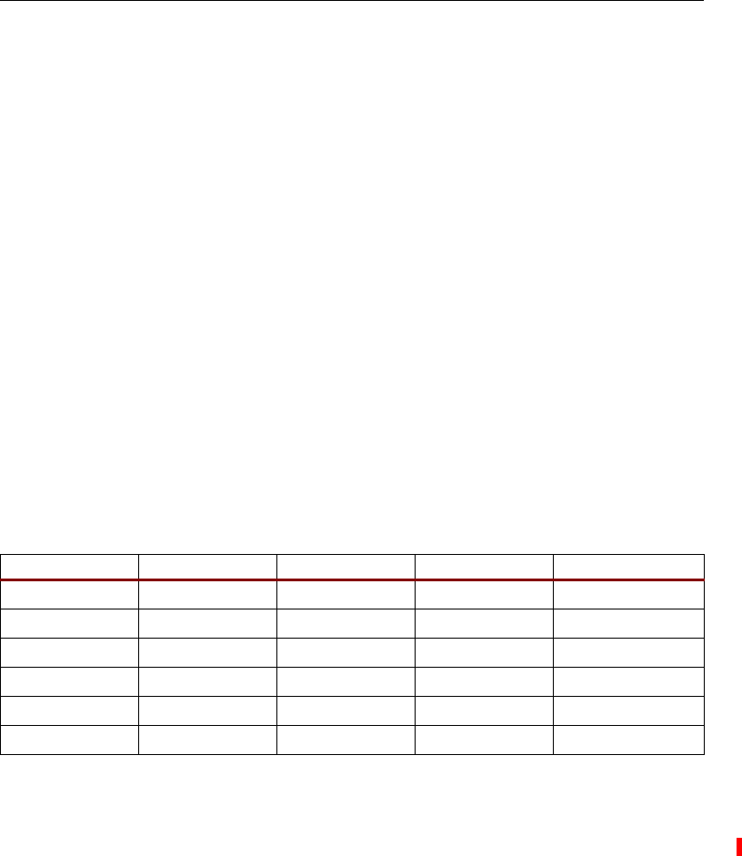
DSP: DESIGNING FOR OPTIMAL RESULTS
96•Xilinx
• Low latency due to the transpose nature of the filter implementation is lower than the Systolic
approach. The latency is equal to the size of one coefficient bank.
The disadvantages to using the Semi-Parallel, Transposed FIR filter are:
• Lower performance due to the broadcast nature of the data buffer output can limit
performance of the filter.
• Control logic is more difficult to understand, but is still of a compact nature.
Rounding
The number of bits on the output of the filter is much larger than the input and must be reduced to a
manageable width. The output can be truncated by simply selecting the MSBs required from the filter.
However, truncation introduces an undesirable DC shift on the data set.
Due to the nature of two’s complement numbers, negative numbers become more negative and
positive numbers also become more negative. The DC shift can be improved with the use of symmetric
rounding, where positive numbers are rounded up and negative numbers are rounded down. The
rounding capability built into the DSP48 slice maintains performance and minimizes the use of FPGA
fabric. This is ingrained in the DSP48 slice via the C input port and also the Carry-In port. Rounding
is achieved in the following manner:
For positive numbers: Binary Data Value +
0.10000… and then truncate
For negative numbers: Binary Data Value +
0.01111... and then truncate
The actual implementation always adds
0.0111… to the data value using the C port input as in
the negative case, and then adds the extra carry in required to adjust for positive numbers. Table 6-5
illustrates some examples of symmetric rounding.
In the instance of the semi-parallel FIR filter, an extra DSP48 slice is required to perform the
rounding functionality. It cannot be ingrained into the final accumulator because the rounding cannot
be done on the final result. If the C input is used and the accumulator is put into three-input add
mode, then rounding is performed on the partial result. The more multipliers in the filter, the worse
the rounding performance because even fewer inner products are included in the result. An extra
DSP48 slice is required to perform the rounding.
Due to the finite nature of the DSP48 slices, it is recommended that the symmetric rounder be
actually implemented in the fabric outside of the slices. The function is small and does not have to run
at a high frequency because the results are running at the much slower input data rate.
Table 6-5: Symmetric Rounding Examples
Decimal Value Binary Value Add Round Truncate: Finish Rounded Value
2.4375
0010.0111 0010.1111 0010
2
2.5
0010.1000 0011.0000 0011
3
2.5625
0010.1001 0011.0001 0011
3
-2.4375
1101.1001 1110.0000 1110
-2
-2.5
1101.1000 1101.1111 1101
-3
-2.5625
1101.0111 1101.1110 1101
-3

SEMI-PARALLEL FIR FILTERS
Xilinx • 97
Performance
It does not make sense to compare the performance of the semi-parallel FIR filter in a Virtex-4 device
with Virtex-II Pro results because completely different techniques are used to build the filters. As a
general statement though, Virtex-4 devices improve the speed of the design, shrink the area, and
reduce power drawn by the filter. All designs assume 18-bit data and 18-bit coefficient widths.
Table 6-6 through Table 6-8 compare the specifications for three filters.
Table 6-6: 4-Multiplier, Memory-Based, Semi-Parallel FIR Filter Specifications
(16-Tap Symmetric)
Parameter Specification
Size
94 slices, 5 DSP48 slices
Performance
458 MHz clock speed, 114.5 MSPS
Power
TBD Watt
Table 6-7: 3-Multiplier, Block-RAM-Based, Semi-Parallel FIR Filter Specifications (300-Tap
Symmetric)
Parameter Specification
Size
38 slices, 4 DSP48 slices, 4 block RAMs
Performance
450 MHz clock speed, 4.5 MSPS
Power
TBD Watt
Table 6-8: 4-Multiplier, Block-RAM-Based, Semi-Parallel Transposed FIR Filter
Specifications (400-Tap Symmetric)
Parameter Specification
Size
46 slices, 4 DSP48 slices, 2 block RAMs
Performance
450 MHz clock speed, 4.5 MSPS
Power
TBD Watt
DSP: DESIGNING FOR OPTIMAL RESULTS
98•Xilinx
Conclusion
Semi-parallel FIR filters probably are the most frequently used filter techniques in Virtex-4 high-
performance DSP applications. Figure 6-12 shows the necessary implementation decisions and
provides guidelines for choosing the required structure based on the filter specifications.
The major lines indicate the guideline thresholds between given implementation techniques. For
instance, the shift to using block RAM is desirable when the number of taps needed to be stored in a
given memory exceeds 32. This correlates to two SRL16Es for the data buffers. If more than two
SRL16Es are used in a data buffer, it will be difficult to reach the high clock rate indicated in Chapter
4, “MAC FIR Filters,” Chapter 5, “Parallel FIR Filters,” and this chapter. However, this is only a
guideline. A great deal depends upon how many slices or block RAMs are remaining in the device, the
power requirements, and the available clock frequencies. A given filter implementation is subjective
because a different set of restrictions is provided by every application and design.
In general, the guidelines provided in the past three chapters should enable designers to make
sensible and efficient decisions when designing filters. These chapters also complete the foundations
required for filter construction in Virtex-4 devices so that more complex, multi-channel and
interpolation or decimation multi-rate filters can be constructed. The supplied referenced designs
further aid in helping to understand and utilize these filters.
Figure 6-12: Selecting the Correct Filter Architecture for Semi-Parallel FIR Filters
Semi-Parallel
Distributed
Memory FIR
Increasing
Number of
Multipliers
Semi-Parallel
BRAM FIR
Systolic FIR (symmetric & non-symmetric)
Block RAM
Distributed Memory
Normal Control
MACC FIR
Number of Coefficients (N)
Log Scale
Sample Rate (MHz)
Log Scale
Embedded
Control
MACC FIR
Distributed
Memory
MACC FIR
Transposed FIR
Symmetric
MACC FIR
UG072_c5_12_082304
10-Multiplier
Semi-Parallel
FIR
1000
500505 20 200
200
500
400
300
50
5
100101
1
0.5
10
100

Xilinx • #
Chapter 7
Multi-Channel FIR Filters
This chapter illustrates the use of the advanced Virtex™-4 DSP features when implementing a
widely used DSP function known as multi-channel FIR filtering. Multi-channel filters are used to
filter multiple input sample streams in a variety of applications, including communications and
multimedia.
The main advantage of using a multi-channel filter is leveraging very fast math elements across
multiple input streams (i.e., channels) with much lower sample rates. This technique increases silicon
efficiency by a factor almost equal to the number of channels.
The Virtex-4 DSP48 slice is one of the new and highly innovative diffused elements that form the
basis of the Application Specific Modular BLock or ASMBL architecture. This modular architecture
enables Xilinx to rapidly and cost-effectively build FPGA platforms by combining different elements,
such as logic, memory, processors, I/O, and of course, DSP functionality targeting specific applications
such as wireless or video DSP.
The Virtex-4 DSP48 slice contains the basic elements of classic FIR filters: a multiplier followed
by an adder, delay or pipeline registers, plus the ability to cascade an input stream (B bus) and an
output stream (P bus) without exiting to a general slice fabric.
The resulting DSP designs can have optional pipelining that permits aggregate multi-channel
sample rates of up to 500 million samples per second, while minimizing power consumption and
external slice logic. In the implementation described in this chapter, multi-channel filtering can be
looked at as time-multiplexed, single-channel filters.
In a typical multi-channel filtering scenario, multiple input channels are filtered using a separate
digital filter for each channel. Due to the high performance of the DSP48 block within the Virtex-4
device, a single digital filter can be used to filter all eight input channels by clocking the single filter
with an 8x clock. This implementation uses 1/8th of the total FPGA resource as compared to
implementing each channel separately.
Multi-Channel FIR Implementation Overview
Top Level
The implementation of a six-channel, eight-tap FIR filter using DSP48 elements is depicted in
Figure 7-1. The design elements used in the implementation include the following:
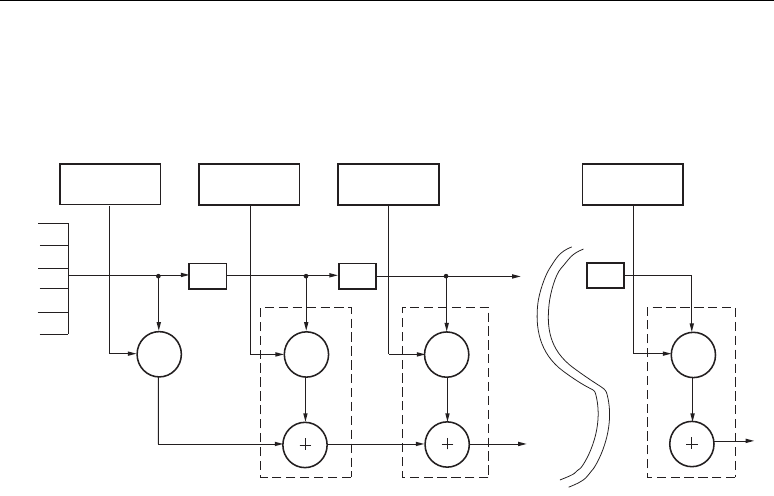
DSP: DESIGNING FOR OPTIMAL RESULTS
# • Xilinx
• Six-to-one multiplexer that is implemented in slice logic as described in “Combining Separate
Input Streams into an Interleaved Stream,” page 101
• Coefficient ROMs using SRL16Es connected in “head-to-tail” fashion
• Input sample “delay-by-seven” SRL16Es to hold the interleaved streams
• DSP48 slices for multiplication and additions
All datapaths and coefficient paths for this example are 8 bits wide. The coefficient ROMs and
input sample delay elements are designed using SRL16Es. The SRL16E is a very compact and efficient
memory element, running at the very high 6x clock rate. For adaptive filtering, where coefficients can
be different depending upon their input signals, coefficient RAMs can be used to update the
coefficient values.
The DSP48 slices and interconnects also run at the 6x clock rate, providing unparalleled
performance for multiplication and additions in today’s FPGAs.
DSP48 Tile
The multi-channel filter block is a cascade implementation of the DSP48 tile. Each tile is
implemented as shown in Figure 7-2. An SRL16E is used to shift the input from the six channels. The
Figure 7-1: Block Diagram of a 6-Channel, 8-Tap FIR Filter
UG073_c6_03_081804
X
X
X
X
x
o
(n)
x
1
(n)
x
2
(n)
x
3
(n)
x
4
(n)
x
5
(n)
Z
-7
Z
-7
Z
-7
SRL16
Coefficient ROM
SRL16
Coefficient ROM
SRL16
Coefficient ROM
SRL16
Coefficient ROM
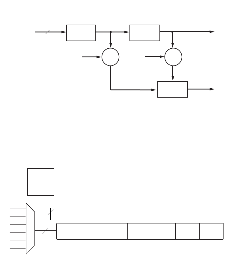
SEMI-PARALLEL FIR FILTERS
Xilinx • 15
product cascade path between two DSP48 slices within the tile can be used to bring the product
output from one tap into the cascading input of the next tap for the final addition.
Combining Separate Input Streams into an Interleaved Stream
As shown in Figure 7-3, six separate video input sample streams must be combined into one
interleaved sample stream for this multi-channel FIR filter example. Conceptually, a high-speed, six-
to-one multiplexer feeds a seven deep SRL16E shift register to accomplish this task. The SRL16E
depth is the number of channels plus one.
For each clock tick, the counter selects a different input stream (in order), and then supplies this
value to the SRL16E shift register. After six clock ticks, the six input samples for a given time period
are loaded sequentially, or interleaved into a single stream.
A six-to-one multiplexer must be designed carefully, as it is constructed with slice logic that must
run at the 6x clock rate. At 446 MHz, good design practices dictate connections “point-to-point,” a
maximum of one Look-Up Table (LUT) between flip-flops and RLOC techniques.
Figure 7-2: DSP48 Tile Cascading Diagram
Figure 7-3: Converting Eight Input Streams to One Interleaved Input Stream
UG073_c6_04_081804
X
C1
8 bits
SRL16
Taps
Input:
6 Channels
Add
SRL16
Taps
C2
X
ug073_c6_05_060904
Shift Register
18
3
Counter
X
5
(n-1)
X
4
(n-1)
X
3
(n-1) X
2
(n-1)
X
1
(n-1) X
0
(n-1)
X
6
(n-1)
DSP: DESIGNING FOR OPTIMAL RESULTS
# • Xilinx
To reduce the high fanouts on the selected lines of the multiplexer, the conceptual multiplexer in
Figure 7-3 is implemented as shown in Figure 7-4. This circuit is repeated for all eight bits of the
input sample width.
Coefficient RAM
The six coefficient sets are stored in the SRL16 memories. If the same coefficient set is used for all
channels, then only a single set is stored in the SRL16. If the different channels use different
coefficients, then six sets of SRL16s are used for each tap. (Six RAMs can be used instead, one for each
channel.)
Each RAM is 8 bits wide and six deep, corresponding to the six taps. The optional Load input is
used to change or load a new coefficient set. Six clock cycles are needed to load all six RAMs. Input C1
is used to load the eight locations of RAM1 which are used for Channel1. C8 is used to load the eight
locations of RAM8 which are used for Channel8. At the eighth clock, all eight locations of the eight
RAMs are loaded; the filter then becomes an adaptive filter. The speed of the overall filter will be
reduced when the coefficients are stored in the RAM.
Control Logic
The control logic is used to ensure proper functioning of the different blocks. If the coefficient RAM
block is used, the control logic ensures that the load signal is High for six clocks. Different tap-
enabled signals are used to make sure that RAM values are read into the DSP48 correctly. For instance,
clock1 reads in the first location from RAM1, but the first location of RAM2 is read only at the clock
number equal to shift register length. The design assumes a clock is running at 6x that of the input
Figure 7-4: High-Speed 8-to-1 Multiplexer Used in the Filter
UG073_c6_06_060904
100000
Shift Register
'0'
'1'
'1'
X
0
(n)
X
1
(n)
LUT
LUT
X
2
(n)
X
3
(n)
LUT
X
4
(n)
X
5
(n)
LUT
LUT
LUT

SEMI-PARALLEL FIR FILTERS
Xilinx • 15
signals. The DCM can also be used to multiply the clock if the only available clock is running at the
input channel frequency.
The control logic also takes care of the initial latency such that the final output is enabled only
after the initial latency period is complete.
Implementation Results
The initial latency of the design is equal to the [(number of channels + 1) * number of taps] plus three
pipe stages within the DSP48. After placement and routing, the design uses 216 slices and eight
DSP48 blocks. The design has a speed of 454 MHz.
Conclusion
The available arithmetic functions within the DSP48 block, combined with fine granularity and high
speed, makes the Virtex-4 FPGA an ideal device to implement high-speed, multi-channel filter
functions. The design shows the efficient implementation of a six-channel, eight-tap filter. Due to the
high-performance capability within the DSP48 block, a single channel, eight-tap filter can be used to
implement the six-channel, eight-tap filter, reducing the area utilization by 1/6th.

DSP: DESIGNING FOR OPTIMAL RESULTS
# • Xilinx


DSP: DESIGNING FOR OPTIMAL RESULTS
# • Xilinx

How Do You Get 256 GigaMAC DSP Performance?
For high-performance DSP design there is no better solution than
XtremeDSP from Xilinx. This book discusses the many advantages
of the Xilinx DSP solution and how to implement working DSP
designs, including:
I The Virtex-4 FPGA family – The ideal platform for creating
high-performance DSP systems and for boosting the performance
of a DSP processor-based system.
I The Virtex-4 technology – Innovative architectural features and
design techniques that dramatically reduce power consumption
while increasing DSP performance.
I The XtremeDSP slice – Optimal performance IP, fully integrated
into the on-chip DSP-specific architecture. (up to 512 XtremeDSP
slices operating at 500 MHz speed.)
I Design tools and support – A broad pallet of easy-to-use design
tools and libraries, in addition to in-depth design support, from
both Xilinx and its partners.
I Education and design services – Get up and running as
quickly as possible.
DSP: Designing for Optimal Results
High-Performance DSP Using Virtex-4 FPGAs
Xcell Publications help you solve design challenges, bringing
you the awareness of the latest tools, devices, and technologies;
knowledge on how to design most effectively; and the next
steps for implementing working solutions. See all of our books,
magazines, technical journals, solutions guides, and brochures
at: www.xilinx.com/xcell
Edition 1.0
April, 2005
DSP Solutions – Advanced Design Guide
